W199 Просмотр технического описания (PDF) - Cypress Semiconductor
Номер в каталоге
Компоненты Описание
Список матч
W199 Datasheet PDF : 14 Pages
| |||
PRELIMINARY
W199
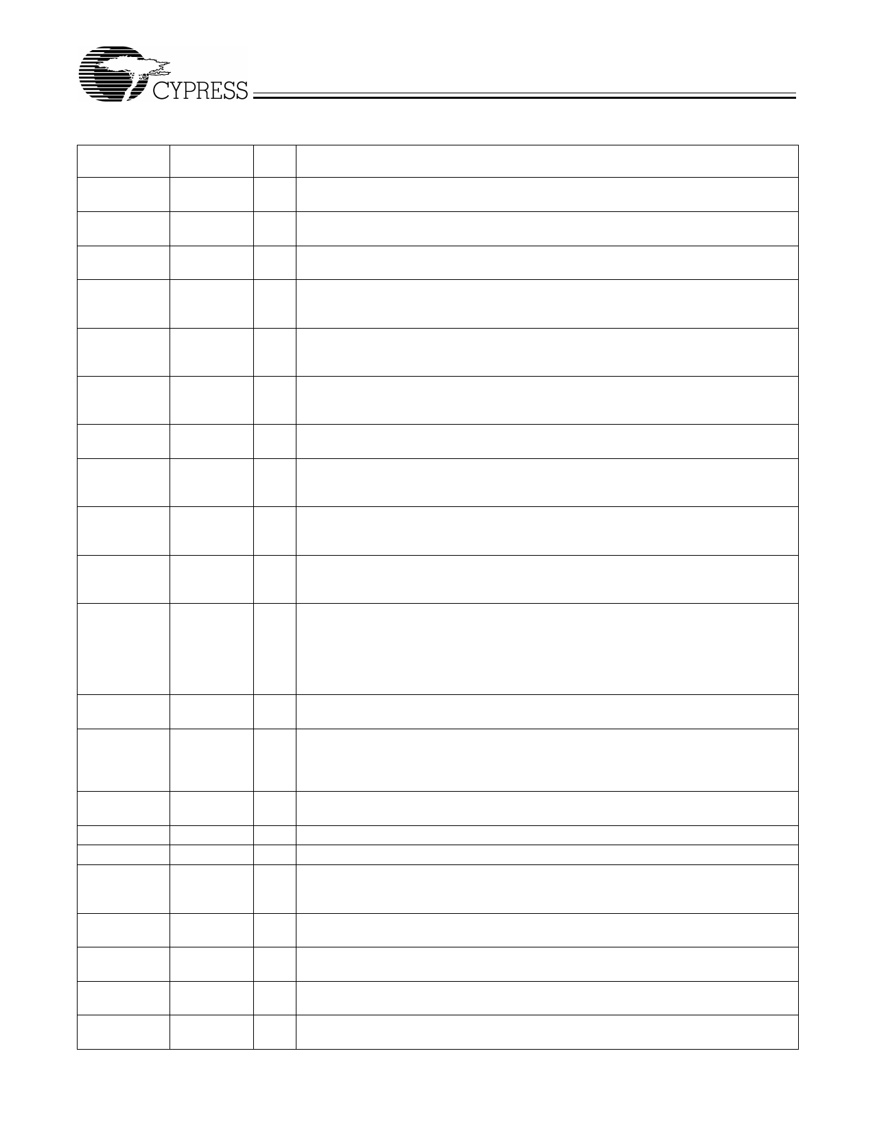
Pin Definitions
Pin Name
CPU_F
Pin No.
44
CPU1
43
PCI2:5
PCI1/FS3
10, 11, 12,
13
8
PCI_F/MODE
7
CLK_STOP#
41
IOAPIC
47
48MHz/FS0
26
24MHz/FS1
25
REF1/FS2
46
REF0/
2
(PCI_STOP#)
SDRAMIN
15
SDRAM0:11
SDRAM_F
38, 37, 35,
34, 32, 31,
29, 28, 21,
20, 18, 17
40
SCLK
24
SDATA
23
X1
4
X2
VDDQ3
VDDQ2
GND
5
1, 6, 14, 19,
27, 30, 36
42, 48
3, 9, 16, 22,
33, 39, 45
Pin
Type
Pin Description
O Free-running CPU Clock: Output voltage swing is controlled by the voltage applied to
VDDQ2. See Tables 2 and 6 for detailed frequency information.
O CPU Clock Output 1: This CPU clock output is controlled by the CLK_STOP# control
pin. Output voltage swing is controlled by voltage applied to VDDQ2.
O PCI Clock Outputs 2 through 5: These four PCI clock outputs are controlled by the
PCI_STOP# control pin. Output voltage swing is controlled by voltage applied to VDDQ3.
I/O Fixed PCI Clock Output: As an output. frequency is set by the FS0:3 inputs or through
serial input interface, see Tables 2 and 6. This output is affected by the PCI_STOP#
input. When an input, latches data selecting the frequency of the CPU and PCI outputs.
I/O Fixed PCI Clock Output: As an output, frequency is set by the FS0:3 inputs or through
serial input interface, see Tables 2 and 6. This output is not affected by the PCI_STOP#
input. When an input, sets function of pin 2.
I CLK_STOP# Input: When brought LOW, affected clock outputs are stopped LOW after
completing a full clock cycle (2–3 CPU clock latency). When brought HIGH, affected
clock outputs start, beginning with a full clock cycle (2–3 CPU clock latency).
O IOAPIC Clock Output: Provides 14.318-MHz fixed frequency. The output voltage swing
is controlled by VDDQ2. This output is disabled when CLK_STOP# is set LOW.
I/O 48-MHz Output: 48 MHz is provided in normal operation. In standard systems, this
output can be used as the reference for the Universal Serial Bus. Upon power-up FS0
input will be latched, which will set clock frequencies as described in Table 2.
I/O 24-MHz Output: 24 MHz is provided in normal operation. In standard systems, this
output can be used as the clock input for a Super I/O chip. Upon power-up FS1 input will
be latched, which will set clock frequencies as described in Table 2.
I/O I/O Dual-Function REF0 and FS2 pin: Upon power-up, FS2 input will be latched which
will set clock frequencies as described in Table 2. When an output, this pin provides a
fixed clock signal equal in frequency to the reference signal provided at the X1/X2 pins.
I/O Fixed 14.318-MHz Output 0 or PCI_STOP# Pin: Function determined by MODE pin.
The PCI_STOP# input enables the PCI 1:5 outputs when HIGH and causes them to
remain at logic 0 when LOW. The PCI_STOP signal is latched on the rising edge of
PCI_F. Its effects take place on the next PCI_F clock cycle. When an output, this pin
provides a fixed clock signal equal in frequency to the reference signal provided at the
X1/X2 pins.
I Buffered Input Pin: The signal provided to this input pin is buffered to 13 outputs
(SDRAM0:11, SDRAM_F).
O Buffered Outputs: These twelve dedicated outputs provide copies of the signal provid-
ed at the SDRAMIN input. The swing is set by VDDQ3, and they are deactivated when
CLK_STOP# input is set LOW.
O Free-running Buffered Output: This dedicated output provides a copy of the SDRAMIN
input which is not affected by the CLK_STOP# input
I Clock pin for I2C circuitry.
I/O Data pin for I2C circuitry.
I Crystal Connection or External Reference Frequency Input: This pin has dual func-
tions. It can be used as an external 14.318-MHz crystal connection or as an external
reference frequency input.
I Crystal Connection: An input connection for an external 14.318-MHz crystal. If using
an external reference, this pin must be left unconnected.
P Power Connection: Power supply for core logic, PLL circuitry, SDRAM outputs, PCI
outputs, reference outputs, 48-MHz output, and 24-MHz output. Connect to 3.3V supply
P Power Connection: Power supply for IOAPIC, CPU_F, and CPU1 output buffers. Con-
nect to 2.5V or 3.3V.
G Ground Connections: Connect all ground pins to the common system ground plane.
2
Share Link: 