CDP1020 Просмотр технического описания (PDF) - Intersil
Номер в каталоге
Компоненты Описание
Список матч
CDP1020 Datasheet PDF : 23 Pages
| |||
CDP1020
LEDG0, LEDA0, LEDG1, LEDA1
The LEDGx and LEDAx are the output LED drive pins for the
device bay status LED located in each bay. The status
indicators should be two color, green/amber, common anode
or anti-parallel LEDs. These pins drive the LEDs directly
through an external current limiting resistor; no additional
buffering is necessary. The high side of these output drivers
is powered directly from the VLED (typically 5V) power input
and is not tied to the VDD rail of the device.
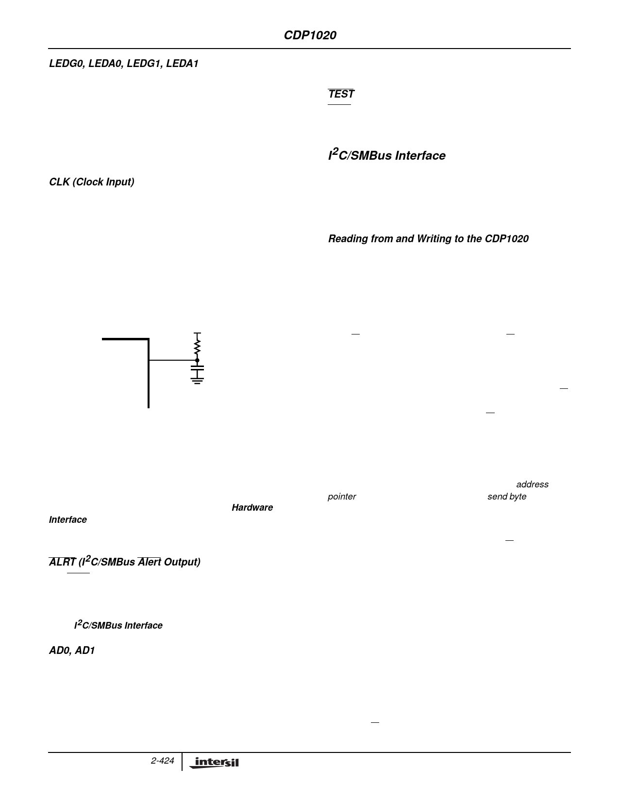
CLK (Clock Input)
The Clock input (CLK) provides the time base reference for
operation of the device bay controller logic, including:
debounce timing, state sequencing, LED timing, etc. SMBus
transfers between the CDP1020 and the SMBus Host
controller are not based on the clock input. The clock input of
the CDP1020 has the circuitry necessary for oscillating an
external resistor-capacitor circuit, as shown in Figure 3.
External clock sources (like those from a can oscillator)
should not be used with the CDP1020.
CLK 26
VDD
CDP1020
FIGURE 3. RC OSCILLATOR CONFIGURATION
The CDP1020 is designed to operate optimally with an input
frequency of 4MHz. All of the internal timing, including
debounce, insertion delay, and solenoid pulse durations are
based on a 4MHz input. While the CDP1020 will operate
over a wide range of frequency, a nominal input frequency of
4MHz is strongly recommended. Refer to the Hardware
Interface text at the end of this document for more
information on the RC oscillator, including recommended RC
values.
ALRT (I2C/SMBus Alert Output)
The ALRT pin is the used by the CDP1020 to signal the
SMBus Host Controller that an interrupt event within the
controller has occurred and the device wishes to be read by
the operating system. This pin is an open drain output. Refer
to the I2C/SMBus Interface text for more details.
.
AD0, AD1
AD0 and AD1 are sampled by the CDP1020 immediately
after reset and are used as the 2 least significant bits of the
I2C/SMBus slave address of the CDP1020. These pins are
CMOS inputs, and should be tied to the same power plane
as the device (VDD for a logic high; VSS for a logic low).
Through the use of these pins, up to four devices may be
placed on the same bus (addresses $90, $92, $94, $96).
TEST
TEST is a CMOS input used only by Intersil for testing, and
is not recommended for the user; it must be externally
connected to VDD.
I2C/SMBus Interface
The CDP1020 contains a standard implementation of an
I2C/SMBus serial interface. The CDP1020 is always an
I2C/SMBus slave device. Its serial interface supports single
or burst mode reads and writes using standard I2C/SMBus
mechanisms.
Reading from and Writing to the CDP1020
The I2C/SMBus slave address of the CDP1020 is
%10010XXY, where the “XX” bits are defined by the
AD1:AD0 input pins, and the “Y” is the R/W (Read/Write) bit.
Every access of the CDP1020 begins when the I2C/SMBus
master generates a start condition (or repeated start
condition) followed by transmitting an address/control byte
with the address equal to the CDP1020’s slave address and
the R/W bit set appropriately. Note that the R/W bit can be
considered the 8th (Least Significant Bit) in the address, even
though that may not be the standard I2C/SMBus notation.
A write operation is defined as the condition when the
I2C/SMBus master transmits the slave address with the R/W
bit clear. A read operation is defined as the transmission of
the CDP1020 slave address with the R/W bit set. Thus,
when looked upon as an 8-bit address, write operations will
have even addresses (for example, $90), while read
operations will be odd ($91).
For write operations, the command byte following the
address/control byte is used to set the internal address
pointer of the CDP1020. An I2C/SMBus send byte command
will therefore behave as a “set the address pointer”
command. The address pointer is initialized to $00 following
a reset. The byte written to the CDP1020 immediately
following an address/control byte with the R/W bit clear will
always be used to set the CDP1020 internal address pointer.
Subsequent bytes written to the CDP1020 in a transmission
following the address/command and address pointer bytes
are written directly into the register space of the CDP1020.
The address pointer of the CDP1020 is auto-incrementing;
once a byte is written into the register space, the address
pointer increments to the next location. In this way multiple
byte writes to adjacent address locations within the
CDP1020 may be performed within a single I2C/SMBus
transmission. Figure 5 shows examples for a single byte and
a multiple byte write to the CDP1020.
Read operations are performed when the I2C/SMBus master
transmits a start condition and the CDP1020 slave address
with the R/W bit set. Following the address/command byte
2-424
Share Link: 