CDP1020 Просмотр технического описания (PDF) - Intersil
Номер в каталоге
Компоненты Описание
Список матч
CDP1020 Datasheet PDF : 23 Pages
| |||
CDP1020
Functional Pin Descriptions
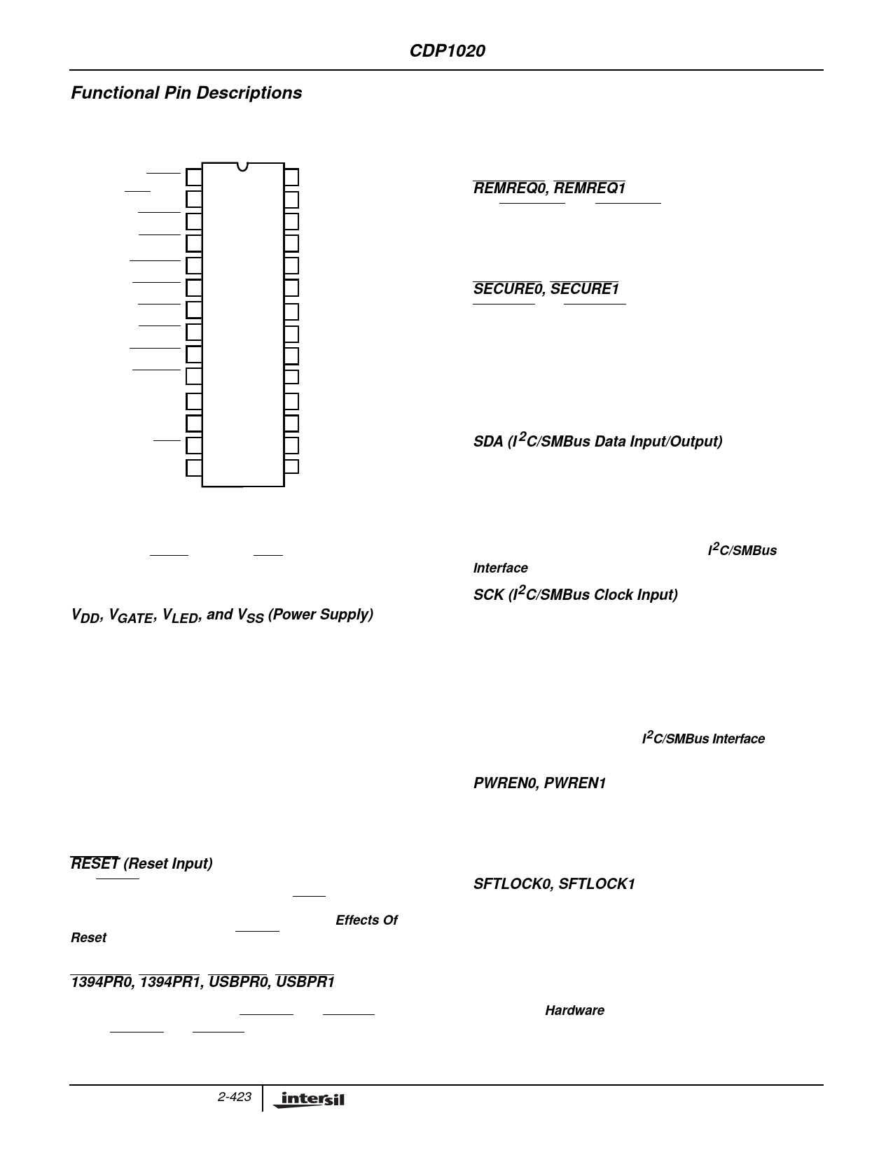
This section provides a description of each of the 28 pins of
the CDP1020 as shown in Figure 2.
RESET 1
TEST (VDD) 2
1394PR0 3
USBPR0 4
REMREQ0 5
SECURE0 6
1394PR1 7
USBPR1 8
REMREQ1 9
SECURE1 10
SDA 11
SCK 12
ALRT 13
VGATE 14
28 AD1
27 AD0
26 CLK
25 VSS
24 VDD
23 VLED
22 LEDA1
21 LEDG1
20 LEDA0
19 LEDG0
18 SFTLOCK1
17 SFTLOCK0
16 PWREN1
15 PWREN0
FIGURE 2. PINOUT DIAGRAM FOR THE CDP1020
NOTE: The following pins are “5V Tolerant” Inputs at all Operating
Voltages: CLK, RESET, SCK, SDA, ALRT. This means that the input
voltages can range up to the maximum allowed (5V typical),
regardless of the operating voltage of the IC.
VDD, VGATE, VLED, and VSS (Power Supply)
Power is supplied to the CDP1020 using these pins. VDD is
connected to the positive logic supply (typically either 3.3V
or 5V), VGATE is connected to the positive supply for the
PWREN0 and PWREN1 gate drivers (typically 12V), VLED is
connected to the positive power supply for the LED drivers
(typically 5V), and VSS is connected to the negative supply
(Ground).
NOTE: VGATE and VLED power supplies should never be connected
to the CDP1020 without the presence of the VDD and VSS supplies.
Applying power to these inputs without the presence of the main
power supply could result in a condition where all level-shifted
outputs (PWRENx, LEDGx and LEDAx) track their power supply
input voltage, thus enabling any of their output circuitry.
RESET (Reset Input)
The RESET input is a low level active input, which resets the
CDP1020. Resetting the device forces ALRT high and forces
the device to reset the state of each bay (see Effects Of
Reset for more details). The RESET pin contains an internal
Schmitt Trigger to improve noise immunity.
1394PR0, 1394PR1, USBPR0, USBPR1
These four pins are the device presence inputs to the device
bay controller for both bay 0 (1394PR0 and USBPR0) and
bay 1 (1394PR1 and USBPR1). If the (peripheral) device
uses the 1394 or USB (or both), that pin(s) on its connector
is tied to GND (active low); when a device is inserted or
removed, these pins are monitored to reflect whether a
device is present (or not), and which of the two busses it
uses. All of these pins are CMOS inputs with internal active
pull-ups to VDD.
REMREQ0, REMREQ1
The REMREQ0 and REMREQ1 inputs are driven from the
“REMOVE REQUEST” buttons for bay 0 and bay 1,
respectively. These pins are CMOS inputs, with internal
active pull-ups to VDD.
SECURE0, SECURE1
SECURE0 and SECURE1 are inputs which are integral to
the bay security feature; each input should be connected
such that it will be asserted when an optional hardware lock
is engaged for the related bay. The state of these inputs are
observable by the operating system through the SL_STS
bits in the bay status registers. Both of these pins are CMOS
inputs with internal active pull-ups to VDD.
SDA (I 2C/SMBus Data Input/Output)
The SDA pin is the serial data input to the SMBus interface
logic of the CDP1020; it contains an internal Schmitt Trigger
to improve noise immunity. When in slave-transmit mode,
this pin is an open drain output. Input thresholds for the SDA
input are fully compliant with SMBus Specification 1.0 (see
Electrical Specifications). Refer to the I2C/SMBus
Interface text for more details.
SCK (I2C/SMBus Clock Input)
The SCK pin is the serial clock input to the SMBus interface
logic of the CDP1020; it contains an internal Schmitt Trigger
to improve noise immunity. Since the CDP1020 never acts
as a SMBus master, this pin is a dedicated clock input
(except for clock-stretching protocol, where it uses an open-
drain low-side output). Input thresholds for the SCK input are
fully compliant with SMBus Specification 1.0 (see Electrical
Specifications). Refer to the I2C/SMBus Interface text for
more details.
PWREN0, PWREN1
PWREN0 and PWREN1 are the outputs from the gate drive
level-shifter circuitry located on the CDP1020. These pins
will output VGATE (typically 12V) to drive the gates of the VID
control MOSFETs per Device Bay Specification 0.90.
SFTLOCK0, SFTLOCK1
SFTLOCK0 and SFTLOCK1 are CMOS outputs designed to
control the software locking mechanism installed in each
bay. These outputs are designed to drive solenoid driver
circuitry (such as an NFET), not a solenoid directly. The
output can be programmed via the Special Function Register
(SFR) to be a level or a pulse of a user defined duration.
Refer to the Hardware text for more details.
2-423
Share Link: 