CDP1020 Просмотр технического описания (PDF) - Intersil
Номер в каталоге
Компоненты Описание
Список матч
CDP1020 Datasheet PDF : 23 Pages
| |||
CDP1020
1394PR0
USBPR0
REMREQ0
SECURE0
LEDA0
LEDG0
PWREN0
SFTLOCK0
DEBOUNCE
LOGIC AND
PULLUP Rs
TIMER/
LEVEL SHIFTER
LEVEL SHIFTER
DEVICE BAY 0
STATE MACHINE
LOGIC
DEVICE BAY 1
STATE MACHINE
LOGIC
DEBOUNCE
LOGIC AND
PULLUP Rs
TIMER/
LEVEL SHIFTER
LEVEL SHIFTER
1394PR1
USBPR1
REMREQ1
SECURE1
LEDA1
LEDG1
PWREN1
SFTLOCK1
SMBUS ALERT
SMBUS ADDRESS BUS
SMBUS DATA BUS
31
0
BSTR0
BCER0
31
0
BSTR1
BCER1
31
15
0
VENDOR ID
REVISION ID
SUBSYS VNDR
SUBSYS REV
DBCCR
SFR
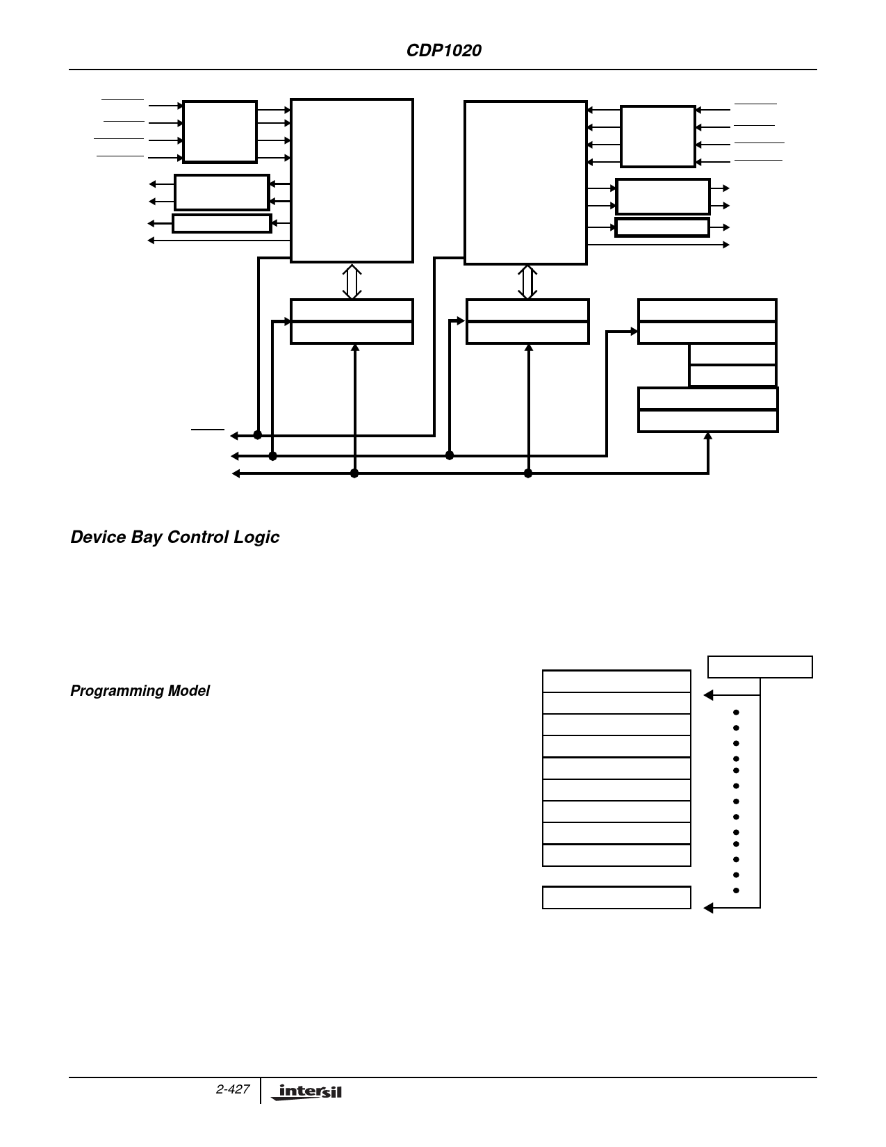
FIGURE 6. CDP1020 CONTROL LOGIC BLOCK DIAGRAM
Device Bay Control Logic
The Device Bay Control Logic unit of the CDP1020 contains
all of the state machine control logic for both device bays, the
register set, debounce logic for the presence and remove
request inputs, and the timer logic for the Device Bay status
LEDs and software lock solenoids. All inputs from the Device
Bays are received from the Input/Output Control Block. A
block diagram of the Control Logic is shown in Figure 6.
Programming Model
There are ten registers within the CDP1020, all of which may
be read by the operating system at any time through the serial
interface. The first nine registers implement the ACPI-based
register set compliant with Device Bay Specification 0.90. The
tenth register (SFR) provides control of other features not
explicitly defined in Device Bay Specification 0.90. A memory
map of the CDP1020 register space is shown in Figure 7.
The second byte transferred at the beginning of every
SMBus write operation defines the address of a byte to
access. Once the address is specified, it is stored in the
CDP1020’s address pointer. Subsequent reads or writes will
access the register selected by the address pointer.
The address pointer will be incremented following each
access facilitating burst mode accesses of sequential bytes
in the CDP1020. Following access of the byte at $FF the
address will increment to $00. Reading of unimplemented
registers will produce undefined results.
Although the CDP1020 memory map is organized into ten
multi-byte registers (8 4-byte registers and 2 2-byte
2-427
registers), the BIOS/operating system is not required to read
or write entire registers. All reads and writes take place at a
byte granularity. For example, to write to the DBCCR, the
BIOS needs to only write a single byte to address location
$0C. The other three bytes of the DBCCR register ($0D:$0F)
do not have to be written to.
$00-03
$04-07
$08-09
$0A-0B
$0C-0F
$10-13
$14-17
$18-1B
$1C-1F
VENDOR ID
REVISION ID
SUBSYSTEM VENDOR ID
SUBSYSTEM ID
DBCCR
BSTR0
BCER0
BSTR1
BCER1
ADDRESS POINTER
$FC-FF
SFR
FIGURE 7. CDP1020 REGISTER SET/MEMORY MAP
NOTE: It is strongly recommended that all write-once-only registers
and bits are programmed after a reset operation, even if the bits
happen to be reset to the desired state, so that a noise transient
during the address of a later write operation doesn’t inadvertently
write new data to any of those locations.
Share Link: 