M65762FP Просмотр технического описания (PDF) - MITSUBISHI ELECTRIC
Номер в каталоге
Компоненты Описание
Список матч
M65762FP Datasheet PDF : 28 Pages
| |||
MITSUBISHI SEMICONDUCTOR (LSI)
M65762FP
QM-CODER
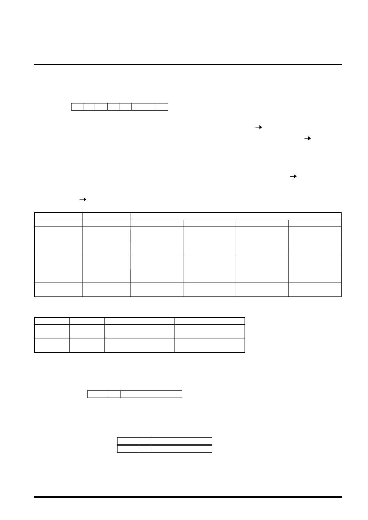
2. Description on Register
(1) System setting register (W/R)
(Address: 0)
d7(MSB)
d0(LSB)
SYS_REG: PB PI BX BS DS CB
HR
d0 (HR): H/W reset (0: Active status, 1: Reset status)
To reset H/W, set this bit to 1 then to 0. The entire LSI
including register group and line memory is initialized
by writing in this reset. However, context table RAM is
not initialized.
d1-2 (CB): Selects the bit width of code data bus (d2 = 0, d1 = 0:
8-bit bus (CD0-7), d2 = 0, d1 = 1: 16-bit bus (CD0-15),
d2 = 1, d1 = 0: 32-bit bus (CD0-31))
(Note1)Prohibition of setting for d2 = 1, d1 = 1
(Note2)For encoding in 16-/32-bit bus, the last
encoding data is output followed by bit byte of
'00' (3 bytes maximum) for word alignment of
encoding data at the end.
d4 (BS):
d5 (BX):
Selection of data bit swap of code data bus (0: MSB
first, 1: LSB first) See Table 2.
Selection of data byte swap of code data bus (0: low
order byte first, 1: high order byte first) See Table 2.
(Note) BX is effective only when the host bus selects
16-bit/32-bit bus.
d6 (PI): Selection of image data input/output I/F (0: serial I/F, 1:
parallel IF)
d7 (PB): Selection of bit width of image data bus (0: 32-bit bus
(PD0-31), 1: 16-bit bus (PD0-15) See Table 3.
Note) PB and DS are effective only when PI = 1.
d3 (DS): Selects data bit swap of image data bus (0: MSB first, 1:
LSB first) See Table 3.
Table 2 Line up of Coded Data/Image Data in Code Data Bus
Bus width (CB)
Swap (BX, BS)
Order of data in code data bus (CD)
d2 d1
d5 d4
CD31 • • CD24
CD23 • • CD16
CD15 • • CD8
10
(32-bits)
00
01
10
11
b24 • • b31
b31 • • b24
b0 • • b7
b7 • • b0
b16 • • b23
b23 • • b16
b8 • • b15
b15 • • b8
b8 • • b15
b15 • • b8
b16 • • b23
b23 • • b16
CD7 • • CD0
b0 • • b7
b7 • • b0
b24 • • b31
b31 • • b24
00
–
01
01
–
10
–
(16-bits)
11
–
–
b8 • • b15
b0 • • b7
–
b15 • • b8
b7 • • b0
–
b0 • • b7
b8 • • b15
–
b7 • • b0
b15 • • b8
00
–0
–
–
–
b0 • • b7
(8-bits)
–1
–
–
–
b7 • • b0
(Note) b0 is image data, given in time series, on the left side of the first encoding data/screen. b31 is image data, given in time series, on the right side of the last encoding data/screen.
Table 3 Order of Image Data on Image Data Parallel Bus
Bit width
Swap
PD31 • • • • PD16
PD15 • • • • PD0
PB=0
DS=0
DS=1
p0 • • • • p15
p31 • • • • p16
p16 • • • • p31
p15 • • • • p0
PB=1
DS=0
–
DS=1
p0 • • • • p15
p15 • • • • p0
p0 is image data on the left side of the screen. p31 is image data on the right side of the screen.
(2) Parameter setting register (W/R)
(Address: 1)
d7 d6 d5 d4
d0
PARA_REG :
AT TM
AT
d0-4 (AT<0>-AT<4>): Low order 5-bits of AT pixel position (See
Figure 2.)
d5 (TM):
Selection of template (0: 3-line template, 1:
2-line template)
d6-7 (AT<5>-AT<6>): High-order 2-bits of AT pixel position
(6th/7th bit)
d7
d4
d0
(Example) 3-line template, AT = 4
00 0 0 0 1 00
2-line template, AT = 48 0 1 1 1 0 0 0 0
(Note) AT pixel position is set (0 to 127) with AT <6:0>.
At the default position (AT pixel is not used), set AT = 0.
The 2-line template, prohibits AT = 1 to 4 from being set. The 3-
line template prohibits AT = 1 to 2 from being set.
Share Link: 