RMWP38001 Просмотр технического описания (PDF) - Fairchild Semiconductor
Номер в каталоге
Компоненты Описание
Список матч
RMWP38001 Datasheet PDF : 8 Pages
| |||
Application Information
CAUTION: THIS IS AN ESD SENSITIVE DEVICE.
Chip carrier material should be selected to have GaAs compatible thermal coefficient of expansion and high thermal
conductivity such as copper molybdenum or copper tungsten. The chip carrier should be machined, finished flat, plated with
gold over nickel and should be capable of withstanding 325°C for 15 minutes.
Die attachment should utilize Gold/Tin (80/20) eutectic alloy solder and should avoid hydrogen environment for PHEMT
devices. Note that the backside of the chip is gold plated and is used as RF and DC ground.
These GaAs devices should be handled with care and stored in dry nitrogen environment to prevent contamination of
bonding surfaces. These are ESD sensitive devices and should be handled with appropriate precaution including the use of
wrist grounding straps. All die attach and wire/ribbon bond equipment must be well grounded to prevent static discharges
through the device.
Recommended wire bonding uses 3 mils wide and 0.5 mil thick gold ribbon with lengths as short as practical allowing for
appropriate stress relief. The RF input and output bonds should be typically 0.012" long corresponding to a typical 2 mil gap
between the chip and the substrate material.
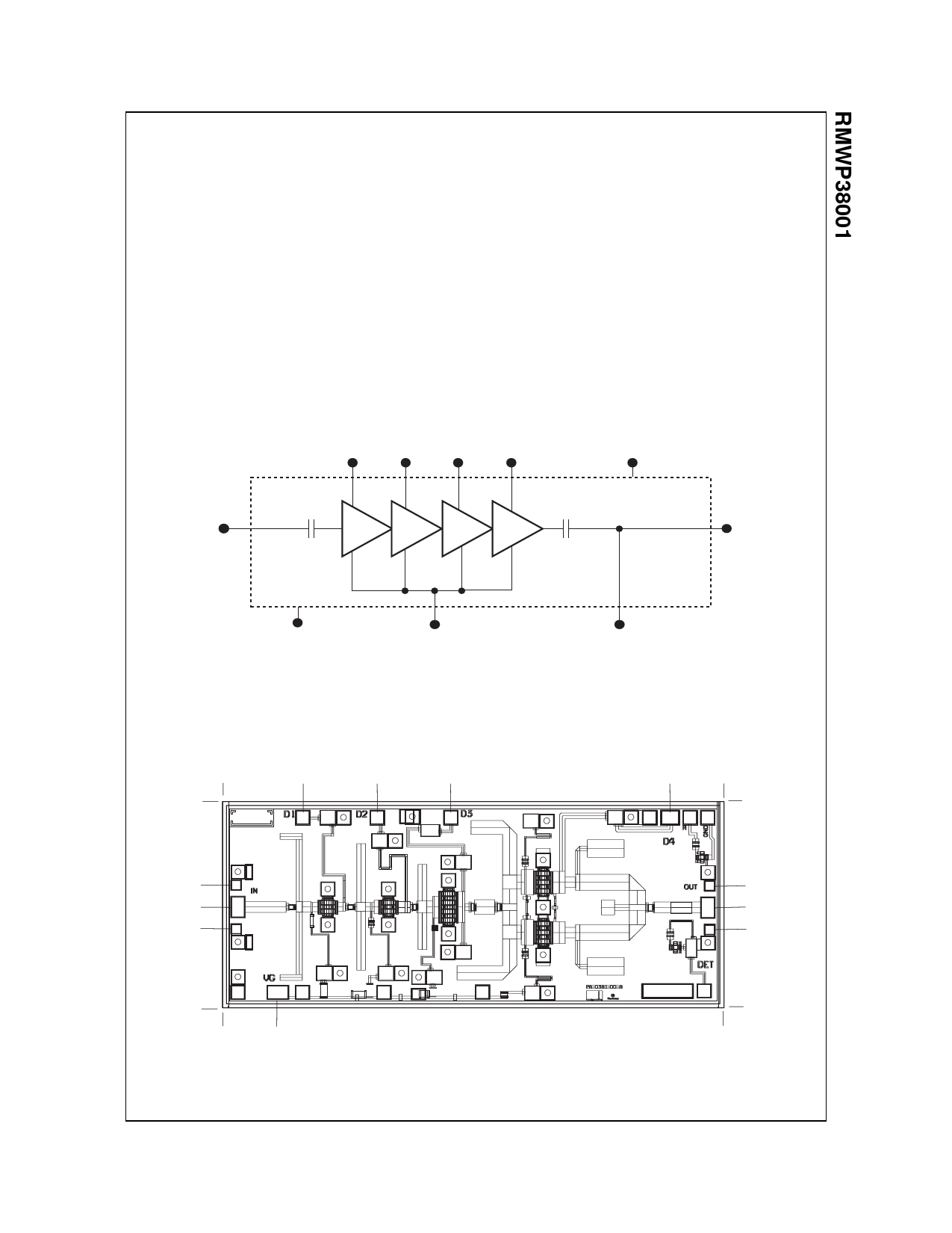
DRAIN DRAIN DRAIN DRAIN
SUPPLY SUPPLY SUPPLY SUPPLY
Vd1
Vd2
Vd3
Vd4
REFERENCE DETECTOR
VOLTAGE Vref
(not connected to circuit)
RF IN
MMIC CHIP
RF OUT
GROUND
(Back of the Chip)
GATE SUPPLY
Vg
OUTPUT POWER DETECTOR
VOLTAGE Vdet
Note:
For output power level detection, bias both detector and reference diodes. DC voltage difference between detector and reference can be used to
measure output power after calibration. If output power level detection is not desired, do not make connection to detector bond pad.
Figure 1. Functional Block Diagram
0.0
1.4
0.545
1.05
1.55
3.0375
3.4
1.4
0.8355
0.686
0.5365
0.8315
0.682
0.5325
0.0
0.0
0.376
Dimensions in mm
Figure 2. Chip Layout and Bond Pad Locations
(Chip Size is 3.4mm x 1.4mm. Back of chip is RF and DC Ground)
0.0
3.4
©2004 Fairchild Semiconductor Corporation
RMWP38001 Rev. C
Share Link: 