ISL97645 Просмотр технического описания (PDF) - Renesas Electronics
Номер в каталоге
Компоненты Описание
Список матч
ISL97645 Datasheet PDF : 14 Pages
| |||
ISL97645
flows continuously in the inductor during the entire switching
cycle in steady state operation. The voltage conversion ratio in
continuous current mode is given by:
V-----BV----oI--N-o---s---t = 1-----–-1----D---
(EQ. 1)
Where D is the duty cycle of the switching MOSFET.
Figure 11 shows the block diagram of the boost regulator. It
uses a summing amplifier architecture consisting of gm stages
for voltage feedback, current feedback and slope
compensation. A comparator looks at the peak inductor current
cycle by cycle and terminates the PWM cycle if the current limit
is reached.
An external resistor divider is required to divide the output
voltage down to the nominal reference voltage. Current drawn
by the resistor network should be limited to maintain the overall
converter efficiency. The maximum value of the resistor
network is limited by the feedback input bias current and the
potential for noise being coupled into the feedback pin. A
resistor network in the order of 60k is recommended. The
boost converter output voltage is determined by the following
equation:
VBoost = R-----1--R---+--2--R-----2- VFB
(EQ. 2)
The current through the MOSFET is limited to 2.6APEAK.
This restricts the maximum output current (average) based on
the following equation:
IOMAX
=
IL
MT
–
---2--I--L-
V-V----I-O-N--
(EQ. 3)
Where IL is peak to peak inductor ripple current, and is set by:
IL = -V---L-I--N-- -fD-s-
(EQ. 4)
where fS is the switching frequency (650kHz or 1.2MHz).
The Table 2 gives typical values (margins are considered 10%,
3%, 20%, 10% and 15% on VIN, VO, L, fS and IOMAX).
Capacitor
An input capacitor is used to suppress the voltage ripple
injected into the boost converter. The ceramic capacitor with
capacitance larger than 10µF is recommended. The voltage
rating of input capacitor should be larger than the maximum
input voltage. Some capacitors are recommended in Table 1
for input capacitor.
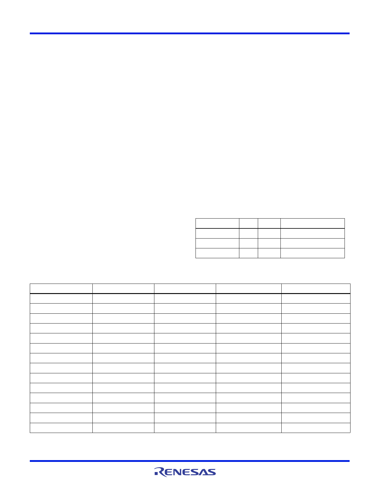
TABLE 1. BOOST CONVERTER INPUT CAPACITOR
RECOMMENDATION
CAPACITOR SIZE MFG
PART NUMBER
10µF/16V
1206 TDK
C3216X7R1C106M
10µF/10V
0805 Murata GRM21BR61A106K
22µF/10V
1210 Murata GRB32ER61A226K
VIN (V)
3
3
3
5
5
5
5
3
3
3
5
5
5
5
TABLE 2. MAXIMUM OUTPUT CURRENT CALCULATION
VO (V)
9
L (µH)
10
Fs (MHz)
0.65
12
10
0.65
15
10
0.65
9
10
0.65
12
10
0.65
15
10
0.65
18
10
0.65
9
10
1.2
12
10
1.2
15
10
1.2
9
10
1.2
12
10
1.2
15
10
1.2
18
10
1.2
IOMAX (mA)
636
419
289
1060
699
482
338
742
525
395
1236
875
658
514
Inductor
The boost inductor is a critical part which influences the output
voltage ripple, transient response, and efficiency. Values of
3.3µH to 10µH are used to match the internal slope
FN9263 Rev 1.00
December 14, 2007
Page 9 of 14
Share Link: 