ISL97645 Просмотр технического описания (PDF) - Renesas Electronics
Номер в каталоге
Компоненты Описание
Список матч
ISL97645 Datasheet PDF : 14 Pages
| |||
ISL97645
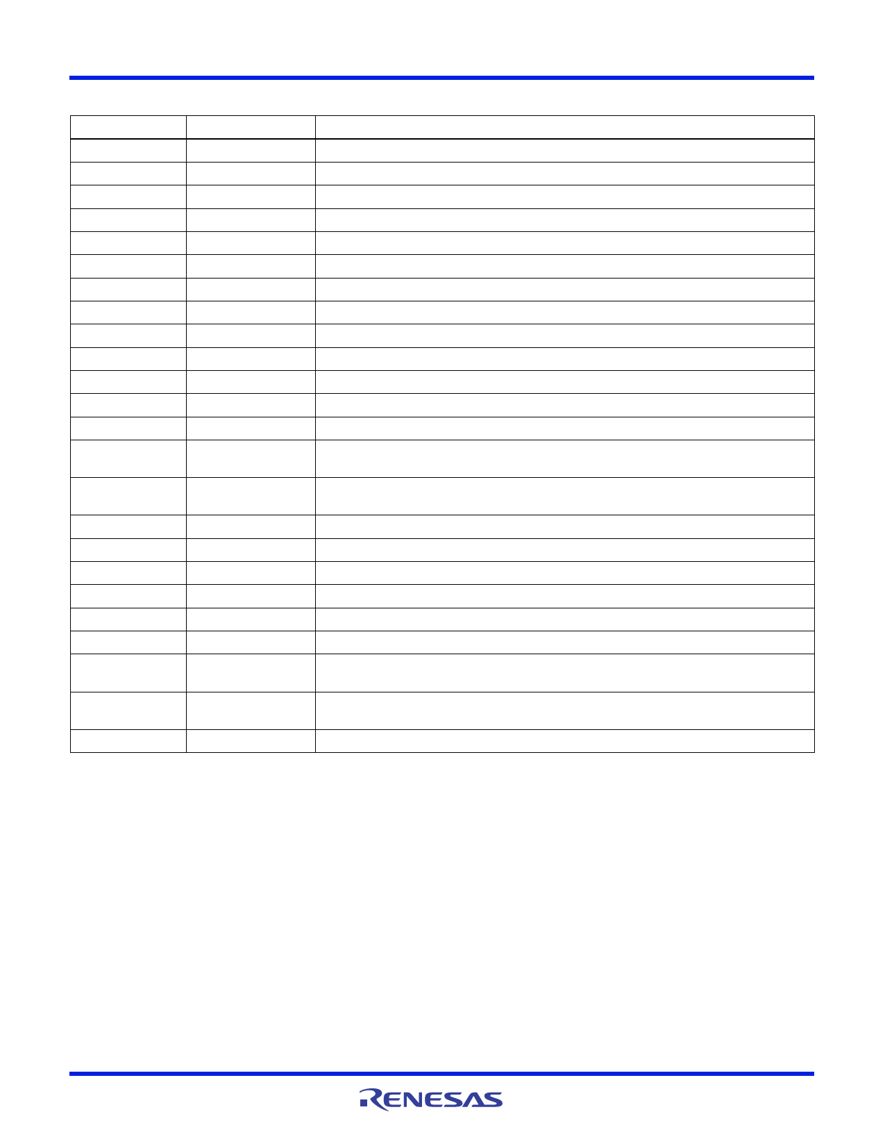
Pin Descriptions
PIN NUMBER
PIN NAME
1
GND
2
VGH_M
3
VFLK
4
VDPM
5
VDD_1
6
VDD_2
7
OUT
8
NEG
9
POS
10
AGND
11
NC
12
NC
13
NC
14
SS
15
COMP
16
FREQ
17
VIN
18
LX
19
ENABLE
20
FB
21
PGND
22
CE
23
RE
24
VGH
FUNCTION
Ground
Gate Pulse Modulation Output
Gate Pulse Modulation Control Input
Gate Pulse Modulation Enable
Gate Pulse Modulation Lower Voltage Input
VCOM Amplifier Supply
VCOM Amplifier Output
VCOM Amplifier Inverting Input
VCOM Amplifier Noninverting Input
VCOM Amplifier Ground
Boost Converter Soft-start. Connect a capacitor between this pin and GND to set the soft-start
time.
Boost Converter Compensation Pin. Connect a series resistor and capacitor between this pin and
GND to optimize transient response.
Boost Converter Frequency Select.
Boost Converter Power Supply
Boost Converter Switching Node
Chip Enable Pin. Connect to Vin for normal operation, GND for shutdown.
Boost Converter Feedback
Boost Converter Power Ground
Gate Pulse Modulator Delay Control. Connect a capacitor between this pin and GND to set the
delay time.
Gate Pulse Modulator Slew Control. Connect a resistor between this pin and GND to set the falling
slew rate.
Gate Pulse Modulator High Voltage Input
FN9263 Rev 1.00
December 14, 2007
Page 2 of 14
Share Link: 