ISL97645 Просмотр технического описания (PDF) - Renesas Electronics
Номер в каталоге
Компоненты Описание
Список матч
ISL97645 Datasheet PDF : 14 Pages
| |||
ISL97645
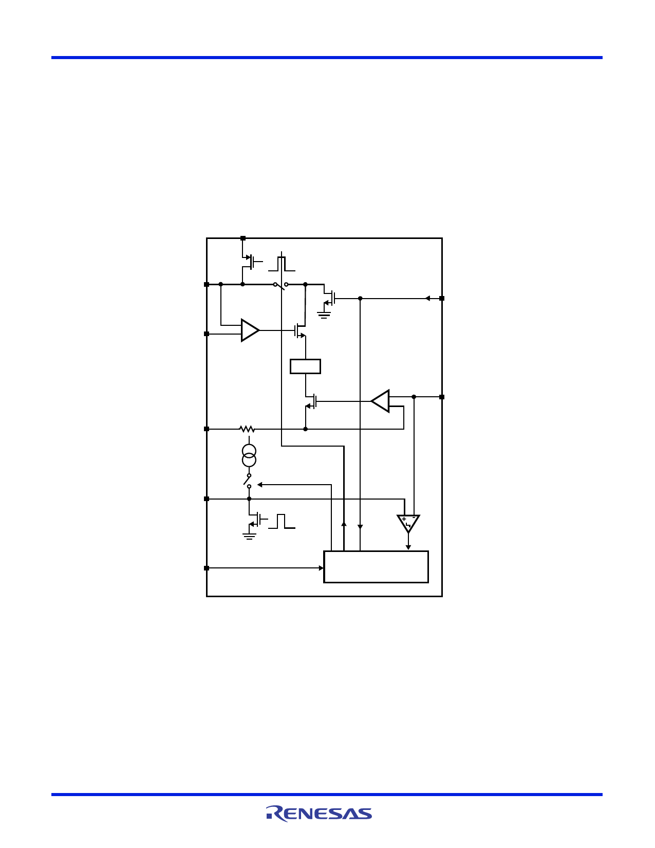
Gate Pulse Modulator Circuit
The gate pulse modulator circuit functions as a three way
multiplexer, switching VGHM between ground, VDD1 and
VGH. Voltage selection is provided by digital inputs VDPM
(enable) and VFLK (control). High to low delay and slew
control is provided by external components on pins CE and
RE, respectively. A block diagram of the gate pulse modulator
circuit is shown in Figure 14.
When VDPM is LOW, the block is disabled and VGHM is
grounded. When VDPM is HIGH, the output is determined by
VFLK. When VFLK goes high, VGHM is pulled to VGH by a
70 switch. When VFLK goes low, there is a delay controlled
by capacitor CE, following which VGHM is driven to VDD1,
with a slew rate controlled by resistor RE. Note that VDD1 is
used only as a reference voltage for an amplifier, thus does not
have to source or sink a significant DC current.
VGH
VGH_M
+
VDD1
-
x240
RE
200µA
CE
EnGPM1
+
VREF
-
VFLK
CONTROL AND
TIMING
FIGURE 14. GATE PULSE MODULATOR CIRCUIT BLOCK DIAGRAM
FN9263 Rev 1.00
December 14, 2007
Page 11 of 14
Share Link: 