ISL97645 Просмотр технического описания (PDF) - Renesas Electronics
Номер в каталоге
Компоненты Описание
Список матч
ISL97645 Datasheet PDF : 14 Pages
| |||
ISL97645
compensation. The inductor must be able to handle the
following average and peak current:
ILAVG = 1----I-–-O----D---
ILPK = ILAVG + ---2--I--L-
(EQ. 5)
Some inductors are recommended in Table 3.
TABLE 3. BOOST INDUCTOR RECOMMENDATION
DIMENSIONS
INDUCTOR
(mm)
MFG
PART NUMBER
6.8µH/3APEAK 7.3x6.8x3.2
10µH/4APEAK 8.3x8.3x4.5
5.2µH/4.55APEAK 10x10.1x3.8
TDK
RLF7030T-6R8N3R0
Sumida CDR8D43-100NC
Cooper CD1-5R2
Bussmann
Rectifier Diode
A high-speed diode is necessary due to the high switching
frequency. Schottky diodes are recommended because of their
fast recovery time and low forward voltage. The reverse
voltage rating of this diode should be higher than the maximum
output voltage. The rectifier diode must meet the output current
and peak inductor current requirements. The following table is
some recommendations for boost converter diode.
TABLE 4. BOOST CONVERTER RECTIFIER DIODE
RECOMMENDATION
DIODE
SS23
VR/IAVG RATING
30V/2A
PACKAGE
MFG
SMB
Fairchild
Semiconductor
MBRS340
40V/3A
SMC
International
Rectifier
SL23
30V/2A
SMB
Vishay
Semiconductor
The following table shows some selections of output
capacitors.
TABLE 5. BOOST OUTPUT CAPACITOR RECOMMENDATION
CAPACITOR SIZE MFG
PART NUMBER
10µF/25V
10µF/25V
1210
1210
TDK
Murata
C3225X7R1E106M
GRM32DR61E106K
Compensation
The boost converter of ISL97645 can be compensated by a
RC network connected from CM1 pin to ground. 4.7nF and 10k
RC network is used in the demo board. The larger value
resistor and lower value capacitor can lower the transient
overshoot, however, at the expense of stability of the loop.
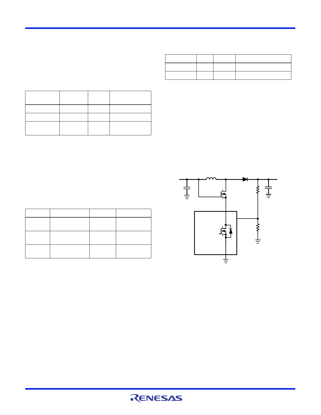
Cascaded MOSFET Application
An 20V N-channel MOSFET is integrated in the boost
regulator. For the applications where the output voltage is
greater than 20V, an external cascaded MOSFET is needed as
shown in Figure 13. The voltage rating of the external
MOSFET should be greater than AVDD.
VIN
AVDD
Intersil
ISL97645
LX
FB
Output Capacitor
The output capacitor supplies the load directly and reduces the
ripple voltage at the output. Output ripple voltage consists of
two components: the voltage drop due to the inductor ripple
current flowing through the ESR of output capacitor, and the
charging and discharging of the output capacitor.
VRIPPLE = ILPK ESR + -V----O---V--–---O--V----I--N-- C-----O-I--O--U----T- -f1-s-
(EQ. 6)
For low ESR ceramic capacitors, the output ripple is dominated
by the charging and discharging of the output capacitor. The
voltage rating of the output capacitor should be greater than
the maximum output voltage.
Note: Capacitors have a voltage coefficient that makes their
effective capacitance drop as the voltage across then
increases. COUT in the equation above assumes the effective
value of the capacitor at a particular voltage and not the
manufacturer’s stated value, measured at zero volts.
FN9263 Rev 1.00
December 14, 2007
FIGURE 13. CASCADED MOSFET TOPOLOGY FOR HIGH
OUTPUT VOLTAGE APPLICATIONS
Page 10 of 14
Share Link: 