LXE1686-0X Просмотр технического описания (PDF) - Microsemi Corporation
Номер в каталоге
Компоненты Описание
Список матч
LXE1686-0X Datasheet PDF : 15 Pages
| |||
LXE1686-0x
INVERTER EVALUATION BOARD
The LXE1686-0x inverter evaluation/design board can
be configured numerous ways for brightness control
by jumper option placement. Basic brightness control
options are as follows:
• Brightness control can be configured for linear DC
input (bypass optional U4 conditioning circuit) with the
following jumper and component changes: RJ3=N/U,
RJ4=N/U, R5=2.0K & C10=220nF
• Brightness control polarity can be reversed such that
a low level input results in maximum brightness by
placing a 10-Ohm jumper at RJ1.
• Brightness control action can be configured as a
direct function of amplitude lamp current (traditional
non-burst mode) by placing a 10-Ohm jumper at RJ2.
• Direct PWM input (wide dynamic range burst mode)
can be configured with the following jumper and
component changes: RJ3=N/U, RJ4=N/U, RJ5=10-
Ohm, RJ6=N/U, RJ7=10-Ohm, VERT SYNC
grounded, R5=2.0K, C5=10-Ohm & C7=10-Ohm
Note that configuration option component and jumper
change items can be found in the ‘Spare
Components’ section of the LXE1686-0x inverter
evaluation/design board. These components; C24
thru C27, R34 thru R35, and RJ9 thru RJ12 can all be
identified on LXE1686 schematic page.
• Direct PWM input is a highly recommended method to
achieve wide dynamic (burst mode) brightness
control, with minimum component count. The
following criteria is required for direct PWM method
brightness control:
• PWM signal logic level amplitude should be no less
than 65% of the VIN LOGIC supply voltage.
• PWM signal frequency should range from 100 to
1000Hz (lower frequency offers wider optical dynamic
dimming range).
• PWM frequency and duty should remain stable and
jitter free during inverter operation.
• PWM signal positive duty should not drop below the
minimum duty that establishes minimum desired
brightness during inverter operation.
• PWM frequency should ideally be synchronized to
application system vertical refresh rate during inverter
operation. This is particularly necessary for STN style
LCD panels, to avoid visual spook interference.
OPTIONAL OPEN LOAD TIME-OUT COMPARATOR CIRCUIT
For safety reasons, inverter design applications may
require high voltage output to be quickly disabled, in
the event of an open load condition (such as a broken
lamp). The LXE1686-0x inverter evaluation/design
board is pre-assembled with an optional comparator
circuit (U5) that provides this function. By placing a
10-Ohm jumper at RJ8, this feature will be fully
enabled for design evaluation. The preset time-out
period is approximately 2 seconds. Vary the RC time
constant values of R33 or C23 if a change in time-out
period is desired.
SHORTED OUTPUT CURRENT LIMITING CIRCUIT
For safety reasons, such as UL (or similar)
requirement, inverter design applications may require
output current to be limited to a specified value, in the
event of a shorted load condition that defeats normal
output current regulation. The LXE1686-0x inverter
evaluation/design board is pre-assembled with a
current limiting sensing circuit (Q1 & R14) that
provides this function. The preset output current
limiting value is approximately 25mA-pk (within UL
requirement). Change the value of R14 (82 Ohm)
inversely for a desired change in output current
limiting.
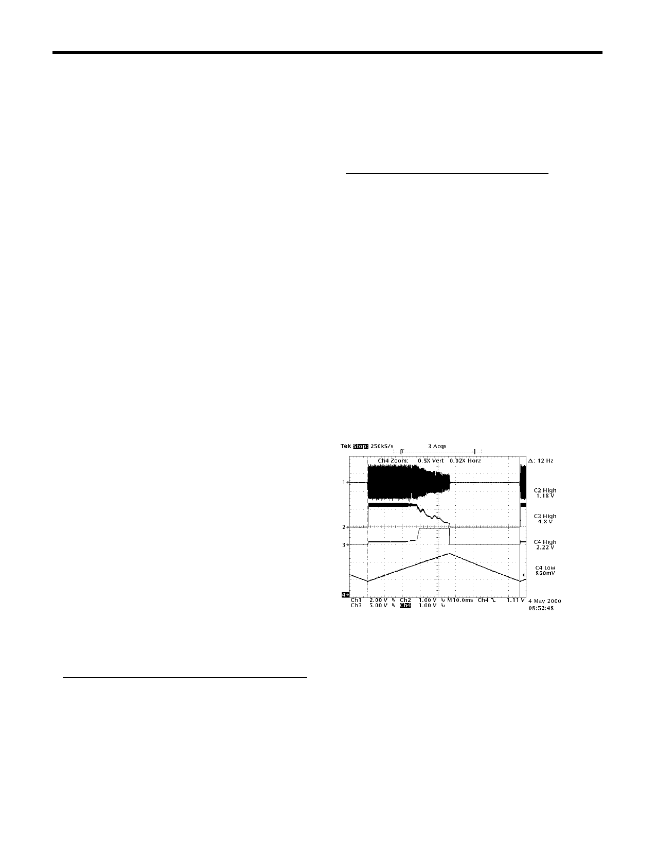
Channel 1 below shows P13 the top on the current
sense resistor. Channel 2 connects to P14 (VSNS),
channel 3 to P15 (VCOMP) and channel 4 to P24
(TRI_C). Since the lamp regulation circuit is defeated
the controller will proceed to the lamp strike
configuration of ramping the output frequency
following the TRI_C ramp generator.
Note that this circuit is not required for normal inverter
operation. It does however; provide protection against
inverter damage as well as user safety, in the event of
a shorted load condition that defeats normal output
current regulation.
4. OSCILLOSCOPE WAVEFORM PICTURES
The following oscilloscope waveform pictures are
provided as a reference to illustrate typical inverter
operating conditions under a typical lamp load, for test
points of visual interest. Variation in waveforms that
Copyright © 2000
Rev 1.0c, 2000-08-31
Page 8
Share Link: 