LXE1686-0X Просмотр технического описания (PDF) - Microsemi Corporation
Номер в каталоге
Компоненты Описание
Список матч
LXE1686-0X Datasheet PDF : 15 Pages
| |||
LXE1686-0x
INVERTER EVALUATION BOARD
VIN POWER
CN1
VIN LOGIC
PWR GND
LINFINITY
LXE1686-0X
F1
U2
C2
U1
TP4
C2A
TIA 7W
T1B 4W
GND
CN2A
CN2A1
PCB CN2B
CAPACITOR CN2B1
+V ENABLE FREQ ADJ
TP2
T1D 2.4W
BRITE CNTL
U3
CURRENT
ADJ TP3
BRITE
ADJ
BRITE RTN
U4
VERT SYNC
GND
TP1
TP1A
BRITE INPUT
CONDITIONING CIRCUIT
U5
TIME-OUT CIRCUIT
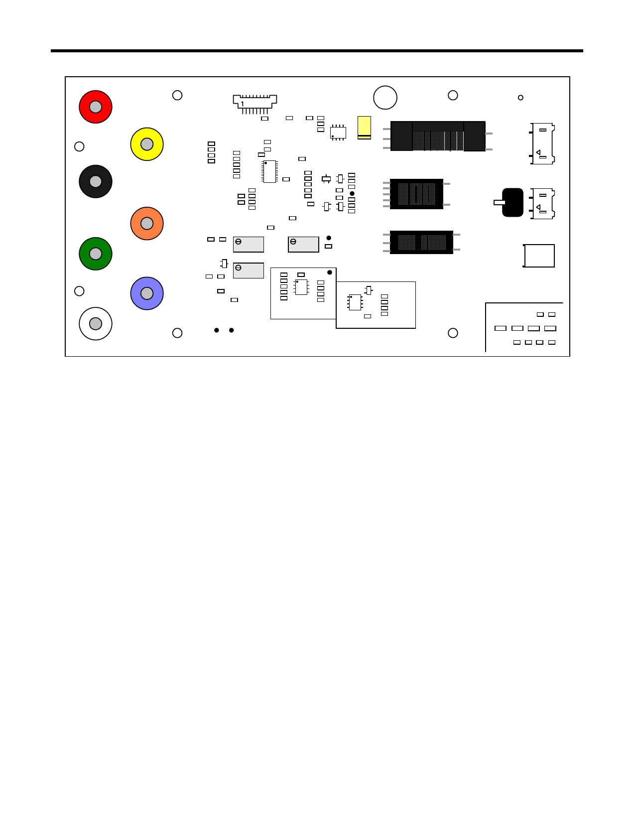
LX1686 INVERTER EVALUATION/DESIGN BOARD
CN2C
CN2C1
SPARE COMPONENTS
DESCRIPTION
The LXE1686-0x CCFL Inverter Evaluation Boards
are designed to demonstrate Linfinity’s LX1686
Backlight Controller IC. It consists of a fully
assembled and tested inverter circuit board. This
design guide complements the LX1686 controller
application note AN-13 that discusses the overall
inverter design considerations. The purpose of the
evaluation board is to allow a designer to quickly
modify the basic inverter circuit to match his LCD
panel requirements. It will allow easy customization
of the inverter’s input and output characteristics to
optimize the inverter design.
LX1686 INVERTER TOPOLOGY
The LX1686 based inverter is a single-stage controller
that regulates lamp current for load and line variation
using a high frequency (60 to 100kHz) PWM
switching technique.
Wide range digital dimming is achieved in a similar
(but separate) manner using a low frequency (100 to
1000Hz) PWM lamp current burst mode technique.
Together, this topology can offer the lowest power
consumption and highest electrical operating
efficiencies achievable from a DC to AC CCFL
inverter.
As with any high performance device, component
load matching is a must to gain the most efficiency
possible. Proper output transformer selection (see
‘Output Transformer Selection’) based on input
voltage and CCFL load should be given careful
consideration, for best inverter performance.
EVALUATION BOARD FEATURES
• Brightness control input conditioning: linear DC,
potentiometer and/or PWM op-amp circuit
• Over-voltage sensing: output voltage limiting, open
load protection circuit
• Over-current sensing: output current limiting,
shorted load/output protection circuit
• Open/short circuit output disabling: timeout output
disabling comparator circuit
• Input interface: full functionality, Banana jacks or 8
pin Molex connector
• Output connector: fly wire or choose from a variety
of most the common industry standards
• Output transformer: choose from three power level
transformer offerings from LINFINITY
LX1686 CONTROLLER FEATURES
• Vertical frame rate synchronization input: pro-
grammable to accept 45 to 500Hz
• Brightness control input: linear DC control input
• Direct PWM dimming input: logic level 100 to
1000Hz PWM, lamp current burst mode
Copyright © 2000
Rev 1.0c, 2000-08-31
Page 2
Share Link: 