LXE1686-0X Просмотр технического описания (PDF) - Microsemi Corporation
Номер в каталоге
Компоненты Описание
Список матч
LXE1686-0X Datasheet PDF : 15 Pages
| |||
LXE1686-0x
INVERTER EVALUATION BOARD
balance is required, the best results usually occur
when R18 and the sum of R11A & R11B are equal in
value.
TP2
ISNS
D2A
BAW56W
P6
LAMP LO
R11A
470
R18
N/U
R11B
5K
C20
3.3NF
OUTPUT VOLTAGE LIMITING, SENSING & MEASUREMENT
The degree of open load or lamp strike potential can
be limited to either the lamp MFR requirement or the
breakdown rating of the magnetic (1800Vrms, for all
three styles). The effective threshold is set by the
ratios of C18 (2.2pF PCB reference) to C19 (2.2nF).
Once again, capacitor tolerance will effect how
accurately TP4 measurement might actually be. The
benefit of this node, as a means of measurement, is
that there is no additional capacitive or resistive
loading to the circuit, as would be associated with a
measurement probe placed directly on the output.
DIMMING CONTROL CIRCUIT CONDITIONING
Capacitor tolerance and circuit response time will
effect how accurately this threshold limit can be
maintained. A safe operating margin should be taken
into consideration for your design expectations. The
recommended pre-assembled component values
noted will limit output to approximately 1500Vrms
(2100Vpk).
If higher strike output potentials are desired but
cannot be achieved, then the maximum strike sweep
frequency may need increasing. This can be
accomplished by reducing the impedance of both R2
(51K) and R3 (9.1K) by approximately the same
percentage. The pre-assembled component values
noted will sweep strike frequency by approximately 3
times the normal operating frequency to excite the
open load resonance of the output transformer.
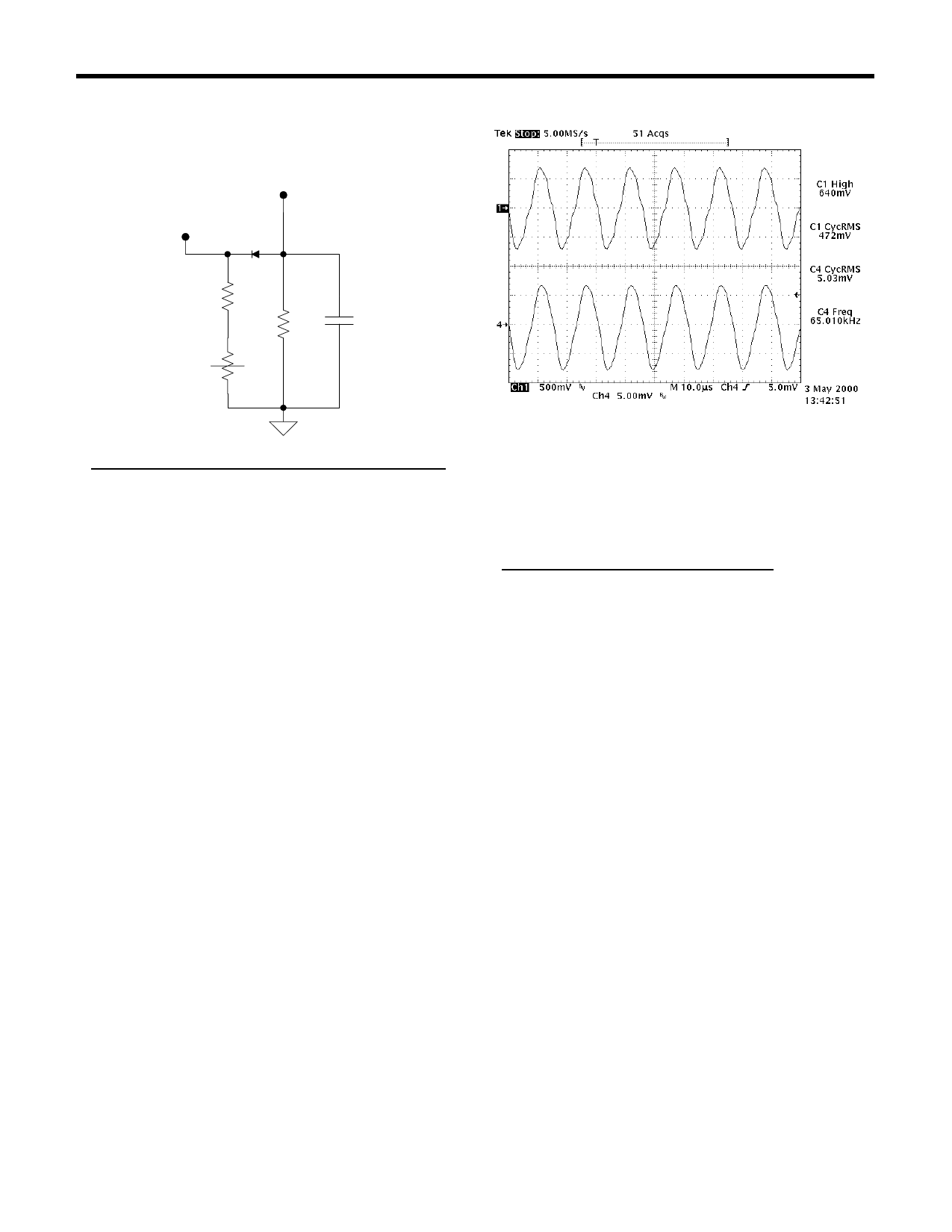
The waveform present at TP4 will closely reflect that
of the high voltage potential presented to the lamp.
TP4 potential is represented as the ratio of C18
(2.2pF PCB reference) to C19 (2.2nF). The pre-
assembled component values noted create an
approximate 1000:1 divider network that could be
used to help determine both open load and normal
run lamp voltage potentials. In the scope picture
below channel 1 is TP4 the center of the 1000:1
capacitive divider and channel four is the lamp low
side run current. This node indicates that the nominal
RMS lamp voltage @ 5mARMS is 472V.
There are many ways to interface inverter dim control
from any given application system. The following
criteria are required at the inverter TP3 ‘BRITE’ input
(with the exception of direct PWM control):
• BRITE signal should have low ripple content, ideally,
less than 10mVpk-pk.
• BRITE signal should have high and low threshold
voltage points that represent desired minimum and
maximum brightness settings.
• Tolerance of the minimum brightness threshold
setting should be relative to the optical dynamic
dimming range desired.
• BRITE signal should not exceed the setting that
establishes minimum desired brightness during
inverter operation.
The LXE1686-0x inverter evaluation/design board is
pre-assembled with a precision voltage reference
(U3) and an op-amp integrator conditioning circuit
(U4) to establish brightness control range with high
and low threshold settings. This circuitry is furnished
as an example of one method to accomplish wide
dynamic range brightness control while accepting
both PWM and or linear DC input signals. Your
application may not require these added components
if the aforementioned design criteria could be met by
some other means.
Copyright © 2000
Rev 1.0c, 2000-08-31
Page 7
Share Link: 