PHB47NQ10T Просмотр технического описания (PDF) - NXP Semiconductors.
Номер в каталоге
Компоненты Описание
Список матч
PHB47NQ10T Datasheet PDF : 13 Pages
| |||
NXP Semiconductors
PHB47NQ10T
N-channel TrenchMOS standard level FET
4. Limiting values
Table 4. Limiting values
In accordance with the Absolute Maximum Rating System (IEC 60134).
Symbol Parameter
Conditions
VDS
VDGR
VGS
ID
drain-source voltage
drain-gate voltage
gate-source voltage
drain current
IDM
peak drain current
Ptot
total power dissipation
Tstg
storage temperature
Tj
junction temperature
Source-drain diode
Tj ≥ 25 °C; Tj ≤ 175 °C
Tj ≥ 25 °C; Tj ≤ 175 °C; RGS = 20 kΩ
VGS = 10 V; Tmb = 100 °C; see Figure 1
VGS = 10 V; Tmb = 25 °C; see Figure 1 and 2
tp ≤ 10 µs; pulsed; Tmb = 25 °C; see Figure 2
Tmb = 25 °C; see Figure 3
IS
source current
ISM
peak source current
Avalanche ruggedness
Tmb = 25 °C
tp ≤ 10 µs; pulsed; Tmb = 25 °C
EDS(AL)S
non-repetitive
VGS = 5 V; Tj(init) = 25 °C; ID = 30 A; Vsup ≤ 25 V;
drain-source avalanche unclamped; tp = 0.1 ms; RGS = 50 Ω; see Figure 4
energy
Min Max Unit
-
100 V
-
100 V
-20 20
V
-
33
A
-
47
A
-
187 A
-
166 W
-55 175 °C
-55 175 °C
-
47
A
-
187 A
-
45
mJ
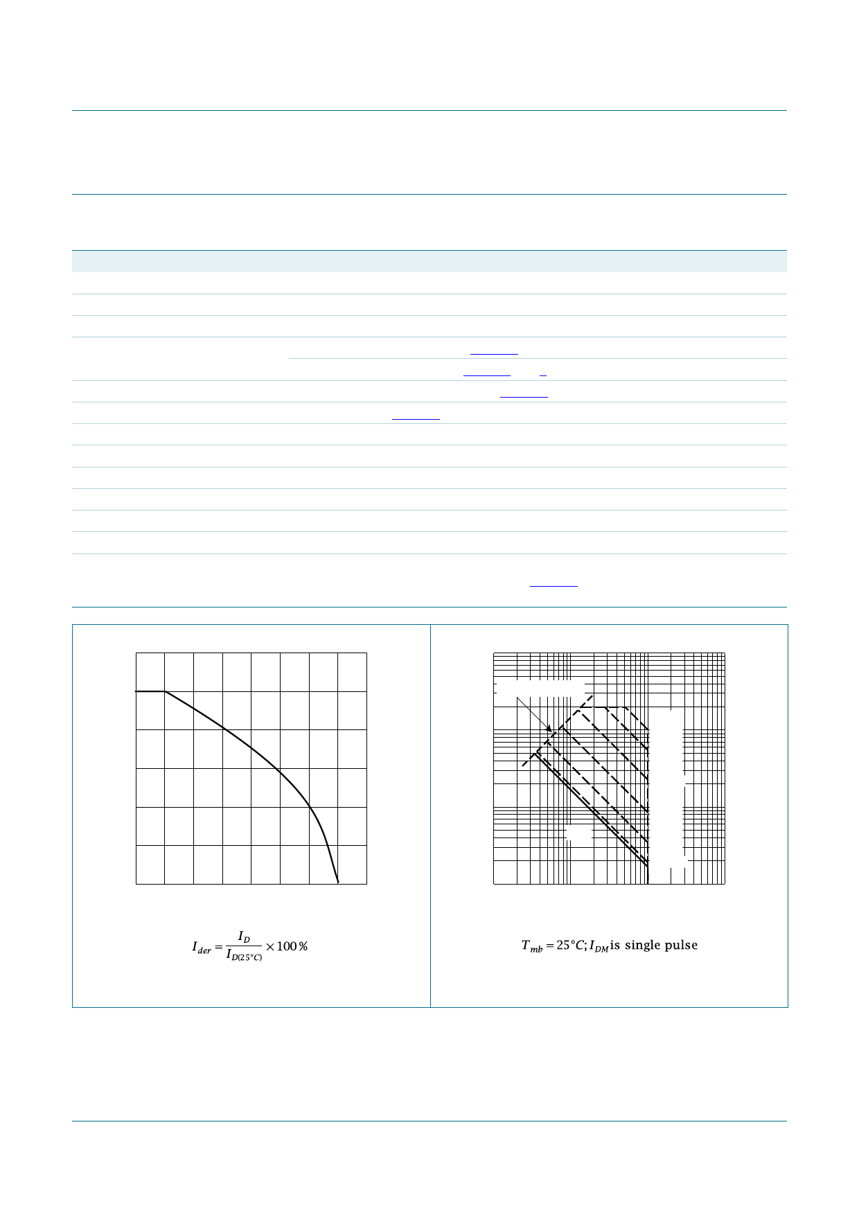
120
Ider
(%)
80
03aa24
40
0
0
50
100
150
200
Tmb (°C)
103
ID
RDSon = VDS / ID
(A)
102
10
D.C.
1
1
10
003aaa097
tp =
1 μs
10 μs
100 μs
1 ms
10 ms
100 ms
102
103
VDS (V)
Fig 1. Normalized continuous drain current as a
function of mounting base temperature
Fig 2. Safe operating area; continuous and peak drain
currents as a function of drain-source voltage
PHB47NQ10T_2
Product data sheet
All information provided in this document is subject to legal disclaimers.
Rev. 02 — 25 February 2010
© NXP B.V. 2010. All rights reserved.
3 of 13
Share Link: 