PTN3460 Просмотр технического описания (PDF) - NXP Semiconductors.
Номер в каталоге
Компоненты Описание
Список матч
PTN3460 Datasheet PDF : 32 Pages
| |||
NXP Semiconductors
PTN3460
eDP to LVDS bridge IC
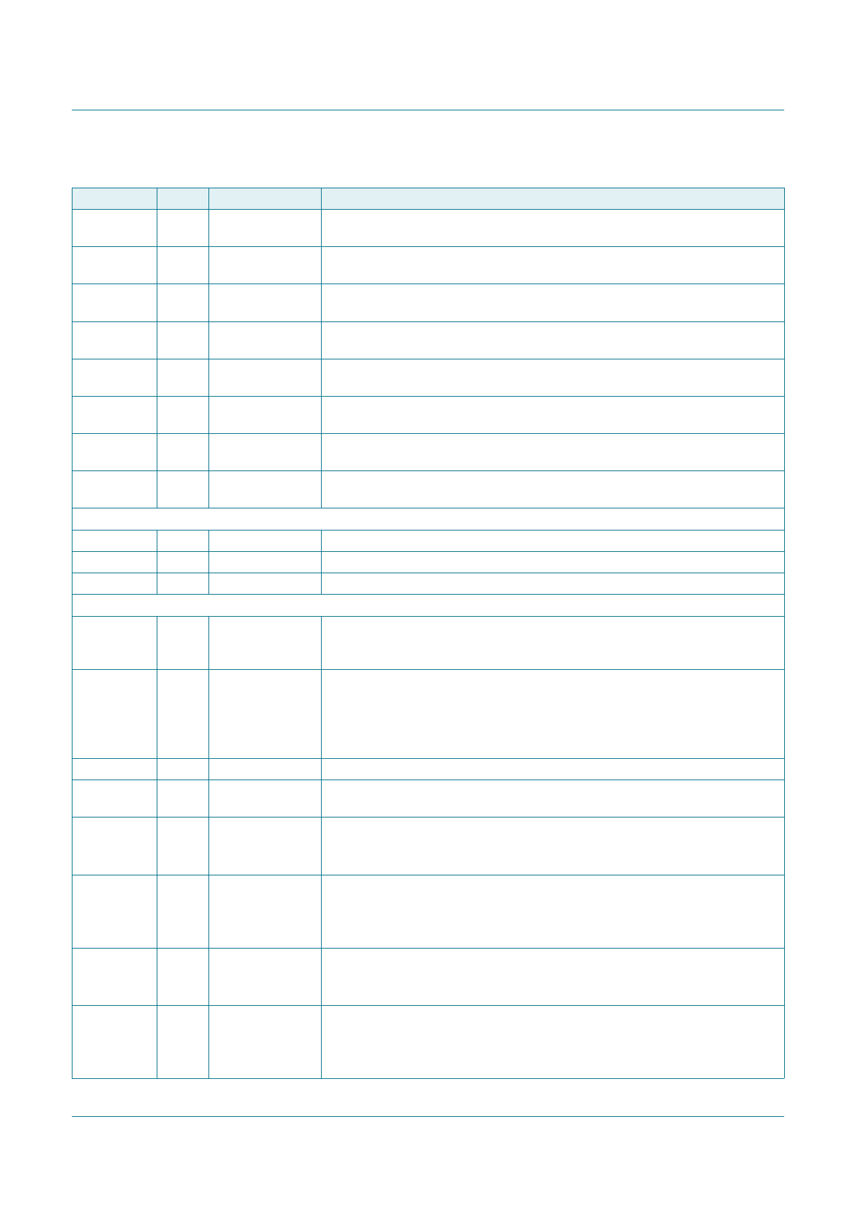
Table 2. Pin description …continued
Symbol
Pin Type
LVSCO_P 48
LVDS output
LVSCO_N 49
LVDS output
LVSCKO_P 46
LVSCKO_N 47
LVSDO_P 43
LVDS clock
output
LVDS clock
output
LVDS output
LVSDO_N 44
LVDS output
DDC_SDA 30
open-drain
DDC data I/O
DDC_SCL 29
open-drain
DDC clock I/O
Panel and backlight interface signals
PVCCEN 33
CMOS output
PWMO
28
CMOS output
BKLTEN
26
CMOS output
Control interface signals
PD_N
10
CMOS input
RST_N
9
CMOS input
DEV_CFG 12
TESTMODE 20
CFG1
21
CMOS I/O
CMOS input
input
CFG2
22
input
CFG3
23
input
CFG4
27
I/O
Description
Odd bus, Channel C differential signal to LVDS receiver. LVSCO_P makes a
differential pair with LVSCO_N.
Odd bus, Channel C differential signal to LVDS receiver. LVSCO_N makes a
differential pair with LVSCO_P.
Odd bus, clock differential signal to LVDS receiver. LVSCKO_P makes a
differential pair with LVSCKO_N.
Odd bus, clock differential signal to LVDS receiver. LVSCKO_N makes a
differential pair with LVSCKO_P.
Odd bus, Channel D differential signal to LVDS receiver. LVSDO_P makes a
differential pair with LVSDO_N.
Odd bus, Channel D differential signal to LVDS receiver. LVSDO_N makes a
differential pair with LVSDO_P.
DDC data signal connection to display panel. Pulled-up by external termination
resistor (5 V tolerant).
DDC clock signal connection to display panel. Pulled-up by external termination
resistor (5 V tolerant).
Panel power (VCC) enable output.
PWM output signal to display panel.
Backlight enable output.
Chip power-down input (active LOW). If PD_N is LOW, then the device is in
Deep power-down completely, even if supply rail is ON; for the device to be able
to operate, the PD_N pin must be HIGH.
Chip reset pin (active LOW); internally pulled-up. The pin is meant to reset the
device and all its internal states/logic; all internal registers are taken to default
value after RST_N is applied and made HIGH.
If RST_N is LOW, the device stays in reset condition and for the device to be
able to operate, RST_N must be HIGH.
I2C-bus address/mode selection pin.
If TESTMODE is left open or pulled HIGH, CFG[4:1] operate as JTAG pins. If
TESTMODE is pulled LOW, these pins serve as configuration pins.
Behavior defined by TESTMODE pin.
If TESTMODE is left open or pulled HIGH, this pin functions as JTAG TEST
CLOCK input. If TESTMODE is pulled LOW, this pin acts as configuration input.
Behavior defined by TESTMODE pin.
If TESTMODE is left open or pulled HIGH, this pin functions as JTAG MODE
SELECT input. If TESTMODE is pulled LOW, this pin acts as configuration
input.
Behavior defined by TESTMODE pin.
If TESTMODE is left open or pulled HIGH, this pin functions as JTAG TEST
DATA INPUT. If TESTMODE is pulled LOW, this pin acts as configuration input.
Behavior defined by TESTMODE pin value.
If TESTMODE is left open or pulled HIGH, this pin functions as JTAG TEST
DATA OUTPUT. If TESTMODE is pulled LOW, this pin acts as configuration
input.
PTN3460
Product data sheet
All information provided in this document is subject to legal disclaimers.
Rev. 4 — 12 March 2014
© NXP Semiconductors N.V. 2014. All rights reserved.
7 of 32
Share Link: 