PTN3460 Просмотр технического описания (PDF) - NXP Semiconductors.
Номер в каталоге
Компоненты Описание
Список матч
PTN3460 Datasheet PDF : 32 Pages
| |||
NXP Semiconductors
PTN3460
eDP to LVDS bridge IC
2.5 General
Power supply: with on-chip regulator
3.3 V 10 % (integrated regulator switched on)
3.3 V 10 %, 1.8 V 5 % (integrated regulator switched off)
ESD: 8 kV HBM, 1 kV CDM
Operating temperature range: 0 C to 70 C
HVQFN56 package 7 mm 7 mm, 0.4 mm pitch; exposed center pad for thermal relief
and electrical ground
3. Applications
AIO platforms
Notebook platforms
Netbooks/net tops
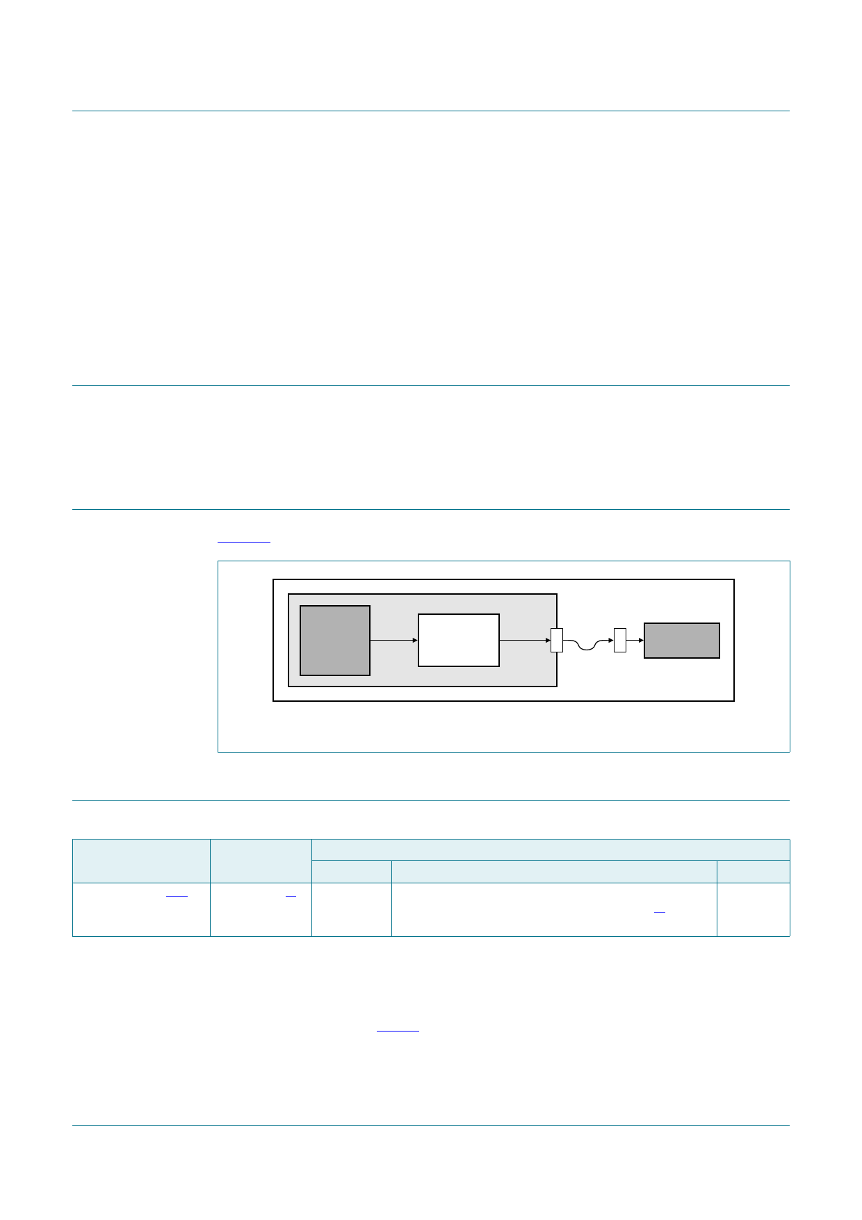
4. System context diagram
Figure 1 illustrates the PTN3460 usage.
CPU/GPU/ eDP
CHIP SET
PTN3460
DP to LVDS
BRIDGE
LVDS
MOTHERBOARD
notebook or AIO platform
cable
LVDS PANEL
Fig 1. PTN3460 context diagram
002aaf831
5. Ordering information
Table 1. Ordering information
Type number
Topside mark
PTN3460BS/Fx[1][2] PTN3460BS[3]
Package
Name
HVQFN56
Description
plastic thermal enhanced very thin quad flat package;
no leads; 56 terminals; body 7 7 0.85 mm[4];
0.4 mm pitch
Version
SOT949-2
[1] PTN3460BS/Fx is firmware-specific, where the ‘x’ indicates the firmware version.
[2] Notes on firmware and marking:
a) Firmware versions are not necessarily backwards compatible.
b) Box/reel labels will indicate the firmware version via the orderable part number (for example, labeling will indicate PTN3460BS/F1 for
firmware version 1). A sample label is illustrated in Figure 8.
[3] Topside marking is limited to PTN3460BS and will not indicate the firmware version.
[4] Maximum package height is 1 mm.
PTN3460
Product data sheet
All information provided in this document is subject to legal disclaimers.
Rev. 4 — 12 March 2014
© NXP Semiconductors N.V. 2014. All rights reserved.
3 of 32
Share Link: 