VT82C586B Просмотр технического описания (PDF) - Unspecified
Номер в каталоге
Компоненты Описание
Список матч
VT82C586B Datasheet PDF : 69 Pages
| |||
9,$7HFKQRORJLHV,QF
VT82C586B
Signal Name
XD7-0,
EXTSMI7-3#,
GPI7-0,
GPO7-0,
Power-up Straps
XDIR
ROMCS# /
KBCS#
Signal Name
GPIO0 /
EXTSMI0#
GPIO1 /
EXTSMI1# /
I2CD1 (Clock)
GPIO2 /
EXTSMI2# /
I2CD2 (Data)
GPIO3 /
EXTSMI3# /
GPI_RE#
GPIO4 /
EXTSMI4# /
GPO_WE
Pin No.
122
121
119
118
117
116
114
113
112
135
Pin No.
94
87
88
92
136
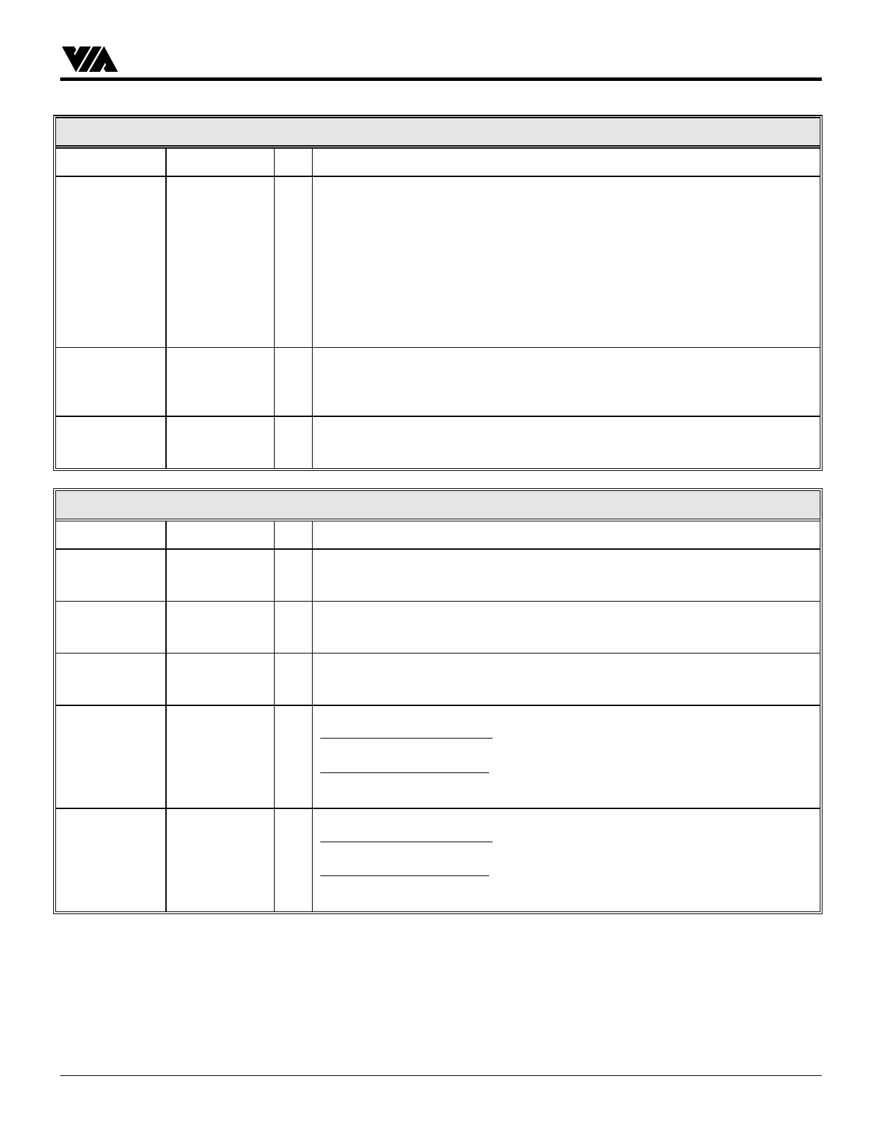
XD Interface
I/O Signal Description
B Multifunction Pins
X-bus Data Bus. For connection to external X-Bus devices (e.g. BIOS ROM)
External SMI Inputs. External SCI/SMI ports.
General Purpose Inputs. GPIO3_CFG bit low (pin 92 = GPI_RE#)
General Purpose Outputs. GPIO4_CFG bit low (pin 136 = GPO_WE)
Power-up Strap Option Inputs. (see Configuration Register Offset 5Ah)
XD0: 0/1 - Disable/enable internal KBC
XD1: 0/1 - Disable/enable internal PS/2 Mouse
XD2: 0/1 - Disable/enable internal RTC
XD4~XD7: RP13~RP16 for internal KBC
O X-Bus Data Direction. XDIR is tied directly to the direction control of a 74F245
transceiver that buffers the X-Bus data and ISA-Bus data (the output enable of the
transceiver should be grounded). SD0-7 connect to the “A” side of the transceiver
and XD0-7 connect to the “B” side. XDIR high indicates that SD0-7 drives XD0-7.
O Multifunction Pin. ROM Chip Select / Keyboard Controller Chip Select.
ISA memory cycle: ROMCS#. Chip Select to the BIOS ROM.
ISA I/O cycle: KBCS#. Chip Select to the external keyboard controller.
General Purpose I/O
I/O Signal Description
B General Purpose I/O 0: General Purpose I/O with external SCI/SMI capability.
This pin sits on the VDD-5VSB power plane and is available even under soft-off
state.
B General Purpose I/O 1: General Purpose I/O with external SCI/SMI capability.
Can be used along with pin 88 as an I2C pair (by software convention this pin is
defined as clock).
B General Purpose I/O 2: General Purpose I/O with external SCI/SMI capability.
Can be used along with pin 87 as an I2C pair (by software convention this pin is
defined as data).
B Multifunction Pin (per GPIO3 Configuration Bit: Function 3 Rx40 bit-6)
GPIO3 Configuration bit high: General Purpose I/O 3: General Purpose I/O with
external SCI/SMI capability.
GPIO3 Configuration bit low: Read Enable for General Purpose Inputs:
Connects to the output enable (OE# pin) of the external 244 buffers whose data pins
connect to SD15-8 and XD7-0 for GPI15-0.
B Multifunction Pin (per GPIO4 Configuration Bit: Function 3 Rx40 bit-7)
GPIO4 Configuration bit high: General Purpose I/O 4: General Purpose I/O with
external SCI/SMI capability.
GPIO4 Configuration bit low: Write Enable for General Purpose Outputs:
Connects to the latch enable (LE pin) of the external 373 latches whose data pins
connect to SD15-8 and XD7-0 for GPO15-0.
Revision 1.0 May 13, 1997
-11-
Pinouts
Share Link: 