UPD72870AF1 Просмотр технического описания (PDF) - NEC => Renesas Technology
Номер в каталоге
Компоненты Описание
Список матч
UPD72870AF1 Datasheet PDF : 52 Pages
| |||
µPD72870A
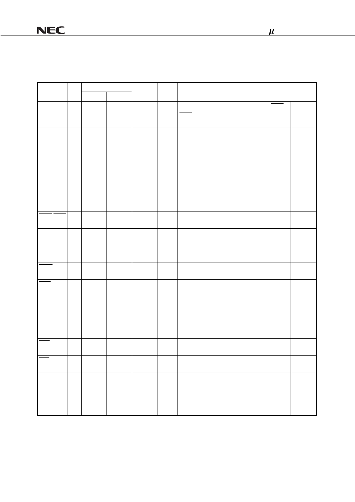
1. PIN FUNCTIONS
1.1 PCI/Cardbus Interface Signals: (52 pins)
Name
I/O
Pin No.
IOL
Volts(V)
Function
LQFP
FBGA
PAR
I/O 45
R4
PCI/Cardbus 5/3.3 Parity is even parity across AD0-AD31 and CBE0-
CBE3. It is an input when AD0-AD31 is an input; it
is an output when AD0-AD31 is an output.
AD0-AD31 I/O 11-14, E1,E2, PCI/Cardbus 5/3.3 PCI Multiplexed Address and Data
16-19, F1,F2,
24-27, G1,G2,
29,30,32, H1,H2,
33,49,50, K1,K2,
52,53, L1,L2,
55-58, M1,M2,
61-64, N1,N2,
66-69
R5-R12,
T5-T12
CBE0-CBE3 I 22,35,47, J2,P2,P9,
-
5/3.3 Command/Byte Enables are multiplexed Bus
60
T4
Commands & Byte enables.
FRAME
I/O 36
P1
PCI/Cardbus 5/3.3 Frame is asserted by the initiator to indicate the
cycle beginning and is kept asserted during the
burst cycle. If Cardbus mode (CARD_ON = 1), this
pin should be pulled up to VDD.
TRDY
I/O 38
R1
PCI/Cardbus 5/3.3 Target Ready indicates that the current data phase
of the transaction is ready to be completed.
IRDY
I/O 37
R2
PCI/Cardbus 5/3.3 Initiator Ready indicates that the current bus
master is ready to complete the current data phase.
During a write, its assertion indicates that the
initiator is driving valid data onto the data bus.
During a read, its assertion indicates that the
initiator is ready to accept data from the currently-
addressed target.
REQ
O8
D1
PCI/Cardbus 5/3.3 Bus_master Request indicates to the bus arbiter
that this device wants to become a bus master.
GNT
I7
D2
-
5/3.3 Bus_master Grant indicates to this device that
access to the bus has been granted.
IDSEL
I 23
J1
-
5/3.3 Initialization Device Select is used as chip select
for configuration read/write transaction during the
phase of device initialization. If Cardbus mode
(CARD_ON = 1), this pin should be pulled up to
VDD.
(1/2)
Link*1
Link
Link
Link
Link
Link
Link
Link
Link
12
Preliminary Data Sheet S14653EJ1V0DS00
Share Link: 