STK12C68 Просмотр технического описания (PDF) - Cypress Semiconductor
Номер в каталоге
Компоненты Описание
Список матч
STK12C68 Datasheet PDF : 24 Pages
| |||
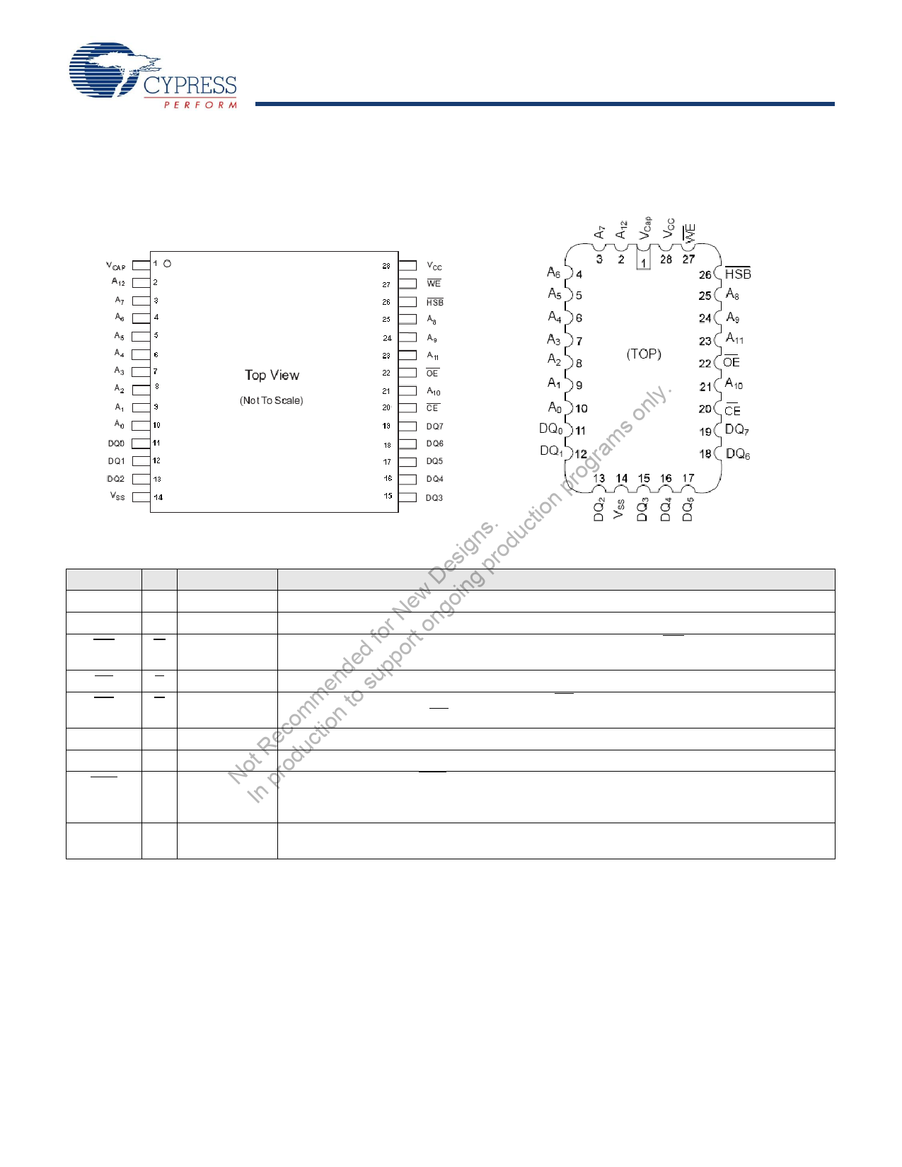
Pin Configurations
Figure 1. 28-Pin SOIC/DIP and LLC
STK12C68
igns. oduction programs only. Pin Definitions
Des pr Pin Name Alt I/O Type
Description
ew oing A0–A12
r N ng DQ0-DQ7
ed fo port o WE
Input
Address Inputs. Used to select one of the 8,192 bytes of the nvSRAM.
Input or Output Bidirectional Data I/O Lines. Used as input or output lines depending on operation.
W
Input
Write Enable Input, Active LOW. When the chip is enabled and WE is LOW, data on the I/O
pins is written to the specific address location.
nd up CE
E
mmen to s OE
G
Input
Input
Chip Enable Input, Active LOW. When LOW, selects the chip. When HIGH, deselects the chip.
Output Enable, Active LOW. The active LOW OE input enables the data output buffers during
read cycles. Deasserting OE HIGH causes the I/O pins to tristate.
eco ctio VSS
t R du VCC
NoIn pro HSB
Ground Ground for the Device. The device is connected to ground of the system.
Power Supply Power Supply Inputs to the Device.
Input or Output Hardware Store Busy (HSB). When LOW, this output indicates a Hardware Store is in progress.
When pulled low external to the chip, it initiates a nonvolatile STORE operation. A weak internal
pull up resistor keeps this pin high if not connected (connection optional).
VCAP
Power Supply AutoStore Capacitor. Supplies power to nvSRAM during power loss to store data from SRAM
to nonvolatile elements.
Document Number: 001-51027 Rev. *C
Page 3 of 24
[+] Feedback
Share Link: 