STK12C68 Просмотр технического описания (PDF) - Cypress Semiconductor
Номер в каталоге
Компоненты Описание
Список матч
STK12C68 Datasheet PDF : 24 Pages
| |||
STK12C68
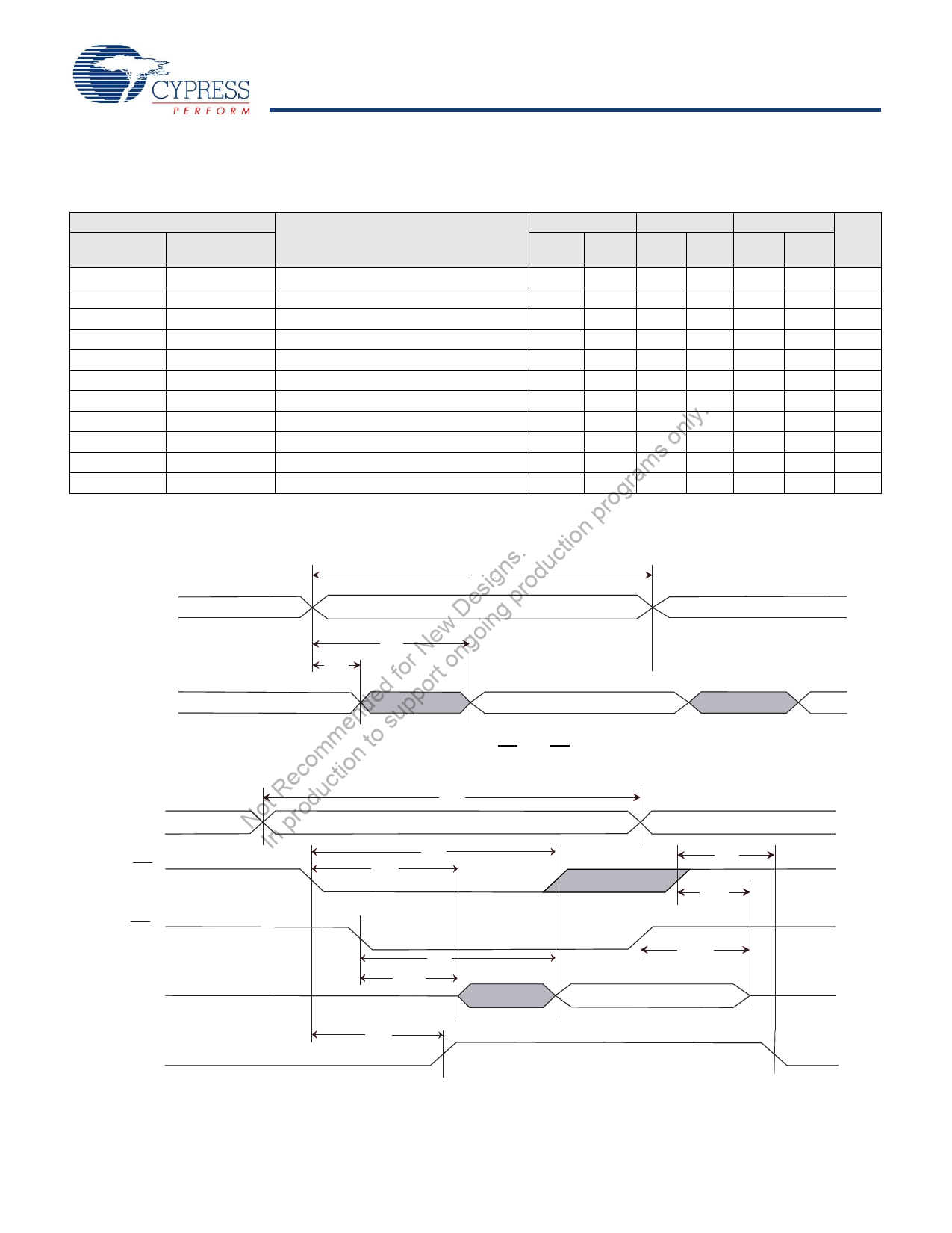
AC Switching Characteristics
SRAM Read Cycle
Parameter
Cypress
Parameter
Alt
Description
25 ns
Min Max
35 ns
Min Max
45 ns
Unit
Min Max
tACE
tRC [7]
tAA [8]
tELQV
tAVAV, tELEH
tAVQV
Chip Enable Access Time
Read Cycle Time
Address Access Time
25
35
45 ns
25
35
45
ns
25
35
45 ns
tDOE
tGLQV
Output Enable to Data Valid
10
15
tOHA [8]
tAXQX
Output Hold After Address Change
5
5
5
tLZCE [9]
tELQX
Chip Enable to Output Active
5
5
5
tHZCE [9]
ly. tLZOE [9]
on tHZOE [9]
s tPU [6]
ram tPD [6]
tEHQZ
tGLQX
tGHQZ
tELICCH
tEHICCL
Chip Disable to Output Inactive
Output Enable to Output Active
Output Disable to Output Inactive
Chip Enable to Power Active
Chip Disable to Power Standby
10
10
0
0
10
10
0
0
25
35
n prog Switching Waveforms
Figure 7. SRAM Read Cycle 1: Address Controlled [7, 8]
igns. ductio W5&
es pro $''5(66
ew Dgoing W$$
r N on W2+$
ed fo port '4
'$7$287
'$7$9$/,'
NoItnRpercoodmucmtieonndto sup $''5(66
Figure 8. SRAM Read Cycle 2: CE and OE Controlled [7]
W5&
W$&(
W3'
0
0
&(
W/=&(
20 ns
ns
ns
12 ns
ns
12 ns
ns
45 ns
W+=&(
2(
'4
'$7$287
W'2(
W/=2(
W+=2(
'$7$9$/,'
W38
$&7,9(
,&&
67$1'%<
Document Number: 001-51027 Rev. *C
Page 10 of 24
[+] Feedback
Share Link: 