MM74HC374 Просмотр технического описания (PDF) - Fairchild Semiconductor
Номер в каталоге
Компоненты Описание
Список матч
MM74HC374 Datasheet PDF : 8 Pages
| |||
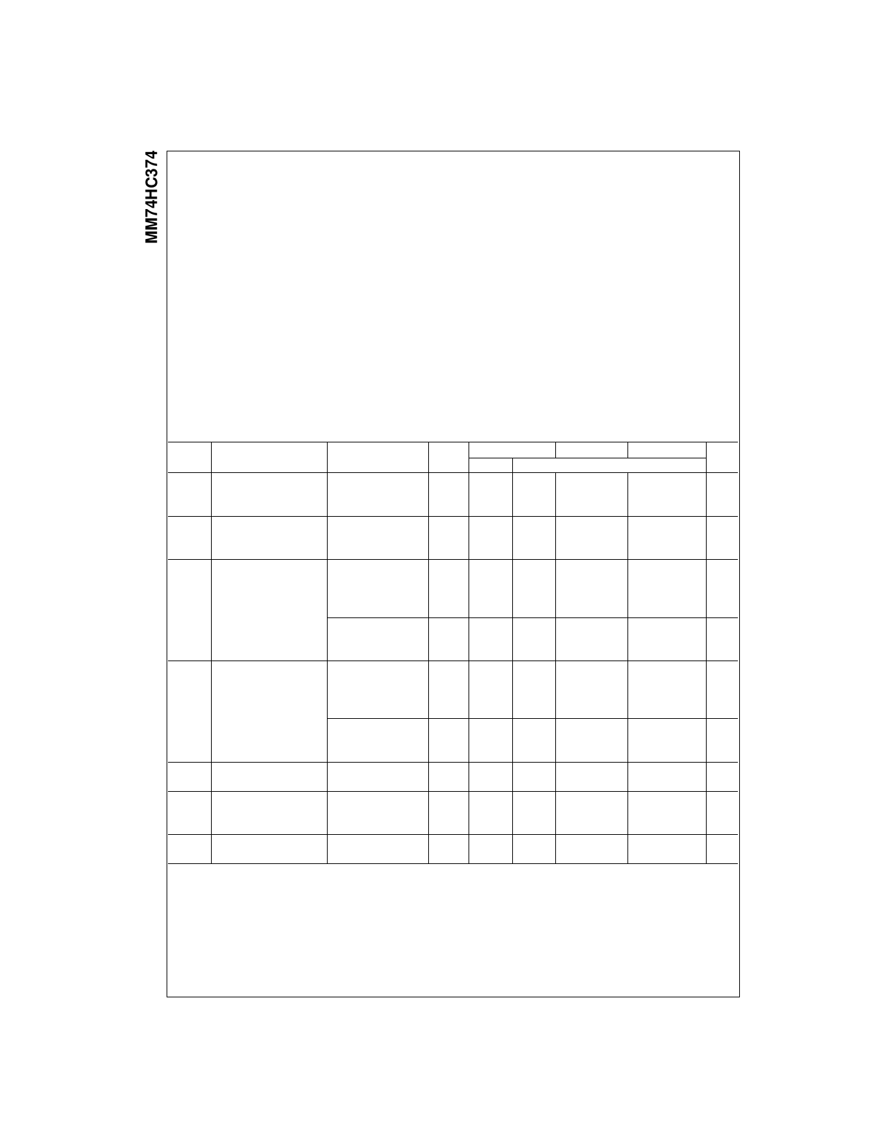
Absolute Maximum Ratings(Note 1)
(Note 2)
Supply Voltage (VCC)
DC Input Voltage (VIN)
DC Output Voltage (VOUT)
Clamp Diode Current (IIK, IOK)
DC Output Current, per pin (IOUT)
DC VCC or GND Current, per pin (ICC)
Storage Temperature Range (TSTG)
Power Dissipation (PD)
(Note 3)
S.O. Package only
Lead Temperature (TL)
(Soldering 10 seconds)
0.5 to 7.0V
1.5 to VCC 1.5V
0.5 to VCC 0.5V
r20 mA
r35 mA
r70 mA
65qC to 150qC
600 mW
500 mW
260qC
Recommended Operating
Conditions
Min Max Units
Supply Voltage (VCC)
DC Input or Output Voltage
2
6
V
(VIN, VOUT)
0
VCC
V
Operating Temperature Range (TA) 40 85
qC
Input Rise or Fall Times
(tr, tf) VCC 2.0V
1000 ns
VCC 4.5V
500
ns
VCC 6.0V
400
ns
Note 1: Absolute Maximum Ratings are those values beyond which dam-
age to the device may occur.
Note 2: Unless otherwise specified all voltages are referenced to ground.
Note 3: Power Dissipation temperature derating — plastic “N” package:
12 mW/qC from 65qC to 85qC.
DC Electrical Characteristics
Symbol
Parameter
Conditions
VCC
TA 25qC
TA 40 to 85qC TA 55 to 125qC Units
Typ
Guaranteed Limits
VIH
Minimum HIGH Level
Input Voltage
2.0V
4.5V
1.5
1.5
3.15
3.15
1.5
V
3.15
V
6.0V
4.2
4.2
4.2
V
VIL
Maximum LOW Level
Input Voltage
2.0V
4.5V
0.5
0.5
1.35
1.35
0.5
V
1.35
V
6.0V
1.8
1.8
1.8
V
VOH
Minimum HIGH Level
Output Voltage
VIN VIH or VIL
|IOUT| d 20 PA
2.0V
2.0
1.9
1.9
4.5V
4.5
4.4
4.4
1.9
V
4.4
V
6.0V
6.0
5.9
5.9
5.9
V
VOL
Maximum LOW Level
Output Voltage
VIN VIH or VIL
|IOUT| d 6.0 mA
|IOUT| d 7.8 mA
VIN VIH or VIL
|IOUT| d 20 PA
4.5V
4.2
3.98
3.84
6.0V
5.7
5.48
5.34
2.0V
0
0.1
0.1
4.5V
0
0.1
0.1
3.7
V
5.2
V
0.1
V
0.1
V
6.0V
0
0.1
0.1
0.1
V
IIN
Maximum Input
Current
VIN VIH or VIL
|IOUT| d 6.0 mA
|IOUT| d 7.8 mA
VIN VCC or GND
4.5V
0.2
0.26
6.0V
0.2
0.26
6.0V
r0.1
0.33
0.33
r1.0
0.4
V
0.4
V
r1.0
PA
IOZ
Maximum 3-STATE
Output Leakage
Current
VIN VIH, OC VIH
VOUT VCC or GND
6.0V
r0.5
r5
r10
PA
ICC
Maximum Quiescent
VIN VCC or GND
6.0V
8.0
80
160
PA
Supply Current
IOUT 0 PA
Note 4: For a power supply of 5V r10% the worst case output voltages (VOH, and VOL) occur for HC at 4.5V. Thus the 4.5V values should be used when
designing with this supply. Worst case VIH and VIL occur at VCC 5.5V and 4.5V respectively. (The VIH value at 5.5V is 3.85V.) The worst case leakage cur-
rent (IIN, ICC, and IOZ) occur for CMOS at the higher voltage and so the 6.0V values should be used.
www.fairchildsemi.com
2
Share Link: 