MM74HC374 Просмотр технического описания (PDF) - Fairchild Semiconductor
Номер в каталоге
Компоненты Описание
Список матч
MM74HC374 Datasheet PDF : 8 Pages
| |||
September 1983
Revised May 2005
MM74HC374
3-STATE Octal D-Type Flip-Flop
General Description
The MM74HC374 high speed Octal D-Type Flip-Flops uti-
lize advanced silicon-gate CMOS technology. They pos-
sess the high noise immunity and low power consumption
of standard CMOS integrated circuits, as well as the ability
to drive 15 LS-TTL loads. Due to the large output drive
capability and the 3-STATE feature, these devices are ide-
ally suited for interfacing with bus lines in a bus organized
system.
These devices are positive edge triggered flip-flops. Data
at the D inputs, meeting the setup and hold time require-
ments, are transferred to the Q outputs on positive going
transitions of the CLOCK (CK) input. When a high logic
level is applied to the OUTPUT CONTROL (OC) input, all
outputs go to a high impedance state, regardless of what
signals are present at the other inputs and the state of the
storage elements.
The 74HC logic family is speed, function, and pinout com-
patible with the standard 74LS logic family. All inputs are
protected from damage due to static discharge by internal
diode clamps to VCC and ground.
Features
s Typical propagation delay: 20 ns
s Wide operating voltage range: 2–6V
s Low input current: 1 PA maximum
s Low quiescent current: 80 PA maximum
s Compatible with bus-oriented systems
s Output drive capability: 15 LS-TTL loads
Ordering Code:
Order Number Package Number
Package Description
MM74HC374WM
M20B
20-Lead Small Outline Integrated Circuit (SOIC), JEDEC MS-013, 0.300" Wide
MM74HC374SJ
M20D
20-Lead Small Outline Package (SOP), EIAJ TYPE II, 5.3mm Wide
MM74HC374MTC
MTC20
20-Lead Thin Shrink Small Outline Package (TSSOP), JEDEC MO-153, 4.4mm Wide
MM74HC374N
N20A
20-Lead Plastic Dual-In-Line Package (PDIP), JEDEC MS-001, 0.300" Wide
Devices also available in Tape and Reel. Specify by appending the suffix letter “X” to the ordering code.
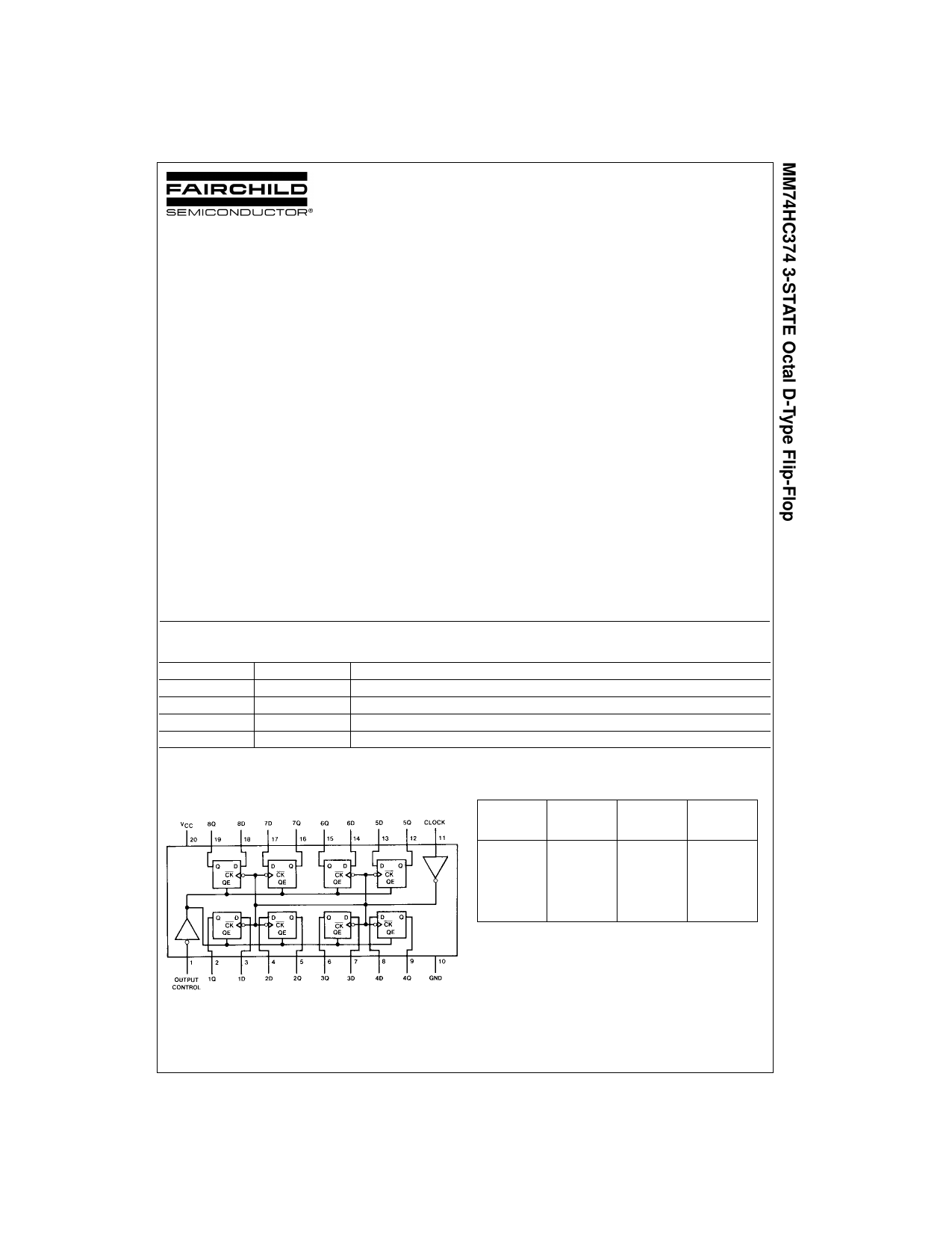
Connection Diagram
Truth Table
Pin Assignments for DIP, SOIC, SOP and TSSOP
Top View
Output
Clock
Data
Output
Control
L
n
H
H
L
n
L
L
L
L
X
Q0
H
X
X
Z
H HIGH Level
L LOW Level
X Don't Care
n Transition from LOW-to-HIGH
Z High Impedance State
Q0 The level of the output before steady state input conditions were
established
© 2005 Fairchild Semiconductor Corporation DS005336
www.fairchildsemi.com
Share Link: 