LH28F320BJE-PTTL90 Просмотр технического описания (PDF) - Sharp Electronics
Номер в каталоге
Компоненты Описание
Список матч
LH28F320BJE-PTTL90 Datasheet PDF : 51 Pages
| |||
SHARP
LHF32JO2
Symbol
TYW
A-1
A,-*20
INPUT
1DQ,-DQ,,
INPUT/
OUTPUT
CE#
INPUT
RP#
INPUT
OE#
INPUT
WE#
INPUT
WI%
INPUT
BYl-E#
INPUT
RY/BY#
OPEN
DRAIN
OUTPUT
Vccw SUPPLY
vcc
GND
SUPPLY
SUPPLY
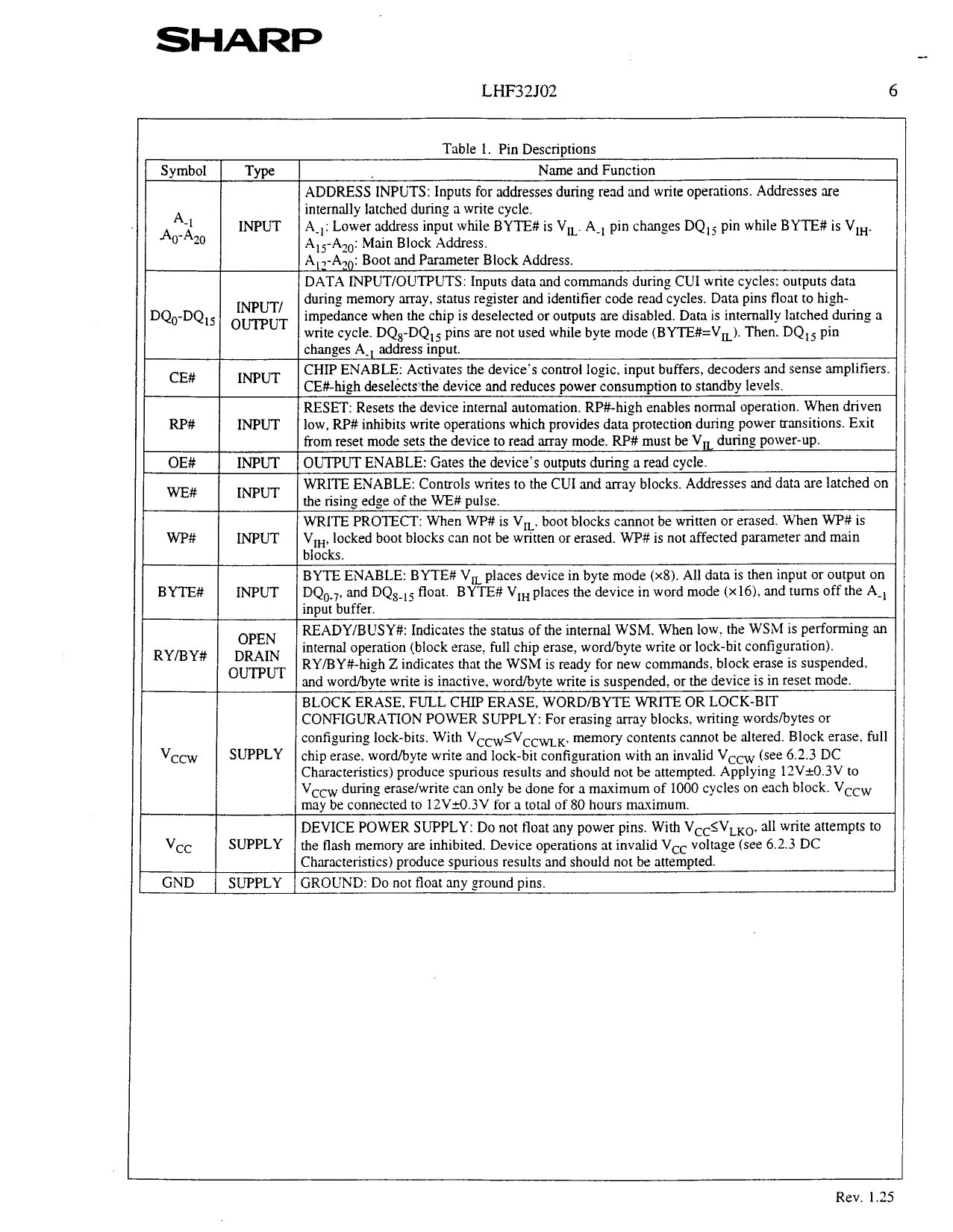
Table 1. Pin Descriptions
Name and Function
ADDRESS INPUTS: Inputs for addresses during read and write operations. Addresses are
internally latched during a write cycle.
A-t: Lower address input while BYTE# is V,,. A-, pin changes DQ, j pin while BYTE# is V,,.
A, j-A20: Main Block Address.
A,1-A20: Boot and Parameter Block Address.
DATA INPUT/OUTPUTS: Inputs data and commands during CUI write cycles: outputs data
during memory array, status register and identifier code read cycles. Data pins float to high-
impedance when the chip is deselected or outputs are disabled. Data is internally latched during a
write cycle. DQ*-DQtj pins are not used while byte mode (BYTE#=V,). Then. DQtj pin
changes A-, address input.
CHIP ENABLE: Activates the device’s control logic, input buffers, decoders and sense amplifiers.
CE#-high deselectsthe device and reduces power consumption to standby levels.
RESET: Resets the device internal automation. RP#-high enables normal operation. When driven
low, RP# inhibits write operations which provides data protection during power transitions. Exit
from reset mode sets the device to read array mode. RP# must be V, during power-up.
OUTPUT ENABLE: Gates the device’s outputs during a read cycle.
WRITE ENABLE: Controls writes to the CUI and array blocks. Addresses and data are latched on
the risine edge of the WE# uulse
WRITE PROTECT: When WP# is V,. boot blocks cannot be written or erased. When WP# is
V,, locked boot blocks can not be written or erased. WP# is not affected parameter and main
blocks.
BYTE ENABLE: BYTE# V, places device in byte mode (x8). All data is then input or output on
DQ,,. and DQs-, j float. BYTE# V,, places the device in word mode (x 16), and turns off the A-t
input buffer.
READY/BUSY#: Indicates the status of the internal WSM. When low, the WSM is performing an
internal operation (block erase, full chip erase, word/byte write or lock-bit configuration).
RY/BY#-high Z indicates that the WSM is ready for new commands. block erase is suspended.
and word/byte write is inactive, word/byte write is suspended, or the device is in reset mode.
BLOCK ERASE, FULL CHIP ERASE, WORD/BYTE WRITE OR LOCK-BIT
CONFIGURATION POWER SUPPLY: For erasing array blocks. writing words/bytes or
configuring lock-bits. With VCCWIVCCWLK. memory contents cannot be altered. Block erase, full
chip erase. word/byte write and lock-bit configuration with an invalid Vccw (see 6.2.3 DC
Characteristics) produce spurious results and should not be attempted. Applying 12V+O.3V to
Vccw during erase/write can only be done for a maximum of 1000 cycles on each block. Vccw
may be connected to 12V&.3V for a total of 80 hours maximum.
DEVICE POWER SUPPLY: Do not float any power pins. With V,,IV,,,, all write attempts to
the flash memory are inhibited. Device operations at invalid V,, voltage (see 6.2.3 DC
Characteristics) produce spurious results and should not be attempted.
GROUND: Do not float any ground pins.
Rev. 1.25
Share Link: 