IDT72V36103 Просмотр технического описания (PDF) - Integrated Device Technology
Номер в каталоге
Компоненты Описание
Список матч
IDT72V36103
Integrated Device Technology

IDT72V36103 Datasheet PDF : 30 Pages
| |||
IDT72V3683/72V3693/72V36103 3.3V CMOS SyncFIFOTM WITH
BUS-MATCHING 16,384 x 36, 32,768 x 36 and 65,536 x 36
COMMERCIAL TEMPERATURE RANGE
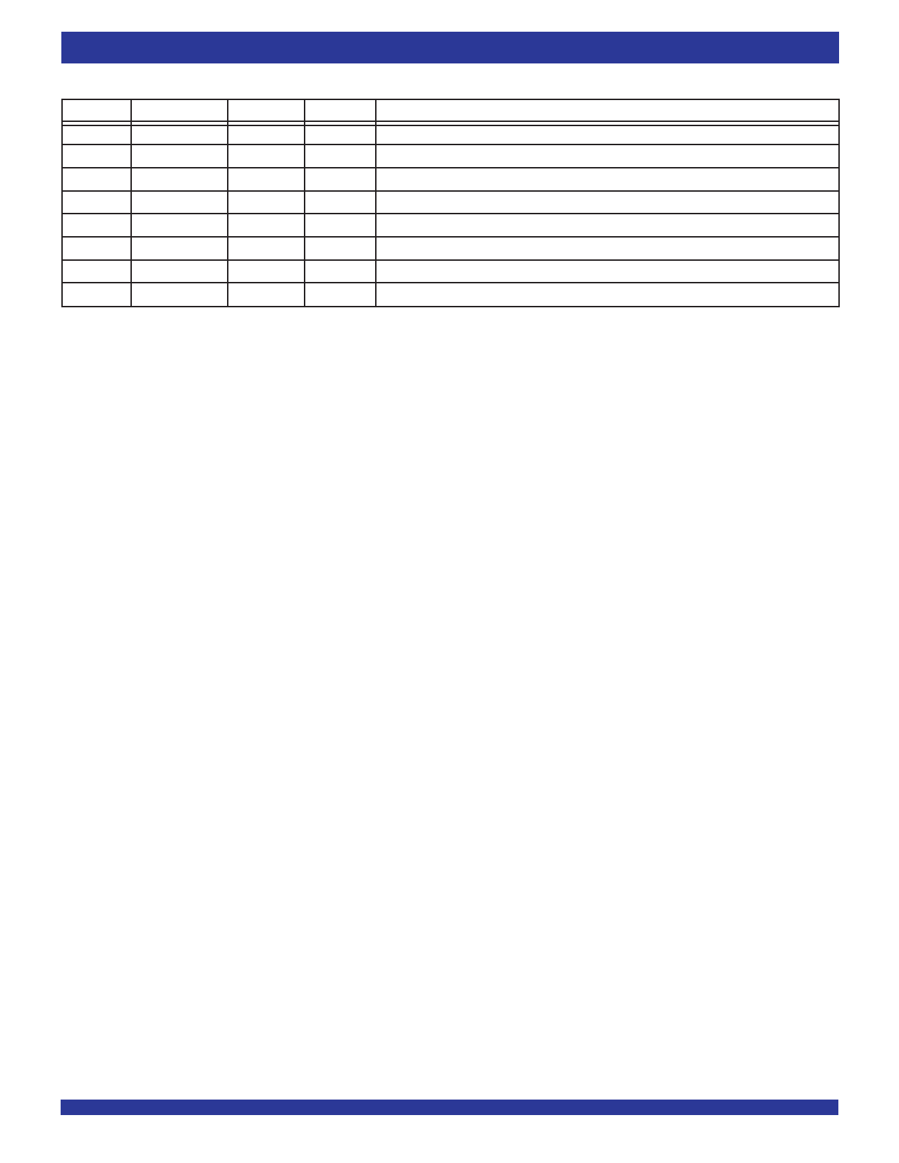
TABLE 1 — FLAG PROGRAMMING
FS2
FS1/SEN
FS0/SD
RS1
X AND Y REGlSTERS(1)
H
H
H
↑
64
H
H
L
↑
16
H
L
H
↑
8
L
H
H
↑
256
L
L
H
↑
1,024
L
H
L
↑
H
L
L
↑
Serial programming via SD
Parallel programming via Port A(2,4)
L
L
L
↑
IP Mode(3,4)
NOTE:
1. X register holds the offset for AE; Y register holds the offset for AF.
2. When this method of parallel programming is selected, Port A will assume Non-Interspersed Parity.
3. When IP Mode is selected, only parallel programming of the offset values via Port A, can be performed and Port A will assume Interspersed Parity.
4. IF parallel programming is selected during a Master Reset, then FS0 & FS1 must remain LOW during FIFO operation.
— PRESET VALUES
To load a FIFO’s Almost-Empty flag and Almost-Full flag Offset registers with
one of the five preset values listed in Table 1, the flag select inputs must be HIGH
or LOW during a reset. For example, to load the preset value of 64 into X and
Y, FS0, FS1 and FS2 must be HIGH when RS1 returns HIGH. For the relevant
preset value loading timing diagram, see Figure 3.
— PARALLEL LOAD FROM PORT A
To program the X and Y registers from Port A, perform a Reset with FS2 HIGH
or LOW and FS0 and FS1 LOW during the LOW-to-HIGH transition of RS1.
The state of FS2 at this point of reset will determine whether the parallel
programming method has Interspersed Parity or Non-Interspersed Parity.
Refer to Table 1 for Flag Programming Flag Offset setup. It is important to note
that once parallel programming has been selected during a Master Reset by
holding both FS0 & FS1 LOW, these inputs must remain LOW during all
subsequent FIFO operation. They can only be toggled HIGH when future
Master Resets are performed and other programming methods are desired.
After this reset is complete, the first two writes to the FIFO do not store data
in RAM. The first two write cycles load the offset registers in the order Y, X. On
the third write cycle the FIFO is ready to be loaded with a data word. See Figure
5, Parallel Programming of the Almost-Full Flag and Almost-Empty Flag
Offset Values after Reset (IDT Standard and FWFT modes), for a detailed
timing diagram. For Non-Interspersed Parity mode the Port A data inputs used
by the Offset registers are (A13-A0), (A14-A0), or (A15-A0) for the IDT72V3683,
IDT72V3693, or IDT72V36103, respectively. For Interspersed Parity mode
the Port A data inputs used by the Offset registers are (A14-A9, A7-A0), (A15-
A9, A7-A0), or (A16-A9, A7-A0) for the IDT72V3683, IDT72V3693, or
IDT72V36103, respectively. The highest numbered input is used as the most
significant bit of the binary number in each case. Valid programming values for
the registers range from 1 to 16,380 for the IDT72V3683; 1 to 32,764 for the
IDT72V3693; and 1 to 65,532 for the IDT72V36103. After all the offset registers
are programmed from Port A, the FIFO begins normal operation.
INTERSPERSED PARITY
Interspersed Parity is selected during a Master Reset of the FIFO. Refer
to Table 1 for the set-up configuration of Interspersed Parity. The Interspersed
Parity function allows the user to select the location of the parity bits in the word
loaded into the parallel port (A0-An) during programming of the flag offset
values. If Interspersed Parity is selected then during parallel programming of
the flag offset values, the device will ignore data line A8. If Non-Interspersed
Parity is selected then data line A8 will become a valid bit. If Interspersed Parity
is selected serial programming of the offset values is not permitted, only parallel
programming can be done.
— SERIAL LOAD
To program the X and Y registers serially, initiate a Reset with FS2 LOW, FS0/
SD LOW and FS1/SEN HIGH during the LOW-to-HIGH transition of RS1. After
this reset is complete, the X and Y register values are loaded bit-wise through
the FS0/SD input on each LOW-to-HIGH transition of CLKA that the FS1/SEN
input is LOW. There are 28-, 30- or 32-bit writes needed to complete the
programming for the IDT72V3683, IDT72V3693 or the IDT72V36103, respec-
tively. The two registers are written in the order Y, X. Each register value can
be programmed from 1 to 16,380 (IDT72V3683), 1 to 32,764 (IDT72V3693)
or 1 to 65,532 (IDT72V36103).
When the option to program the offset registers serially is chosen, the Full/
Input Ready (FF/IR) flag remains LOW until all register bits are written. FF/IR
is set HIGH by the LOW-to-HIGH transition of CLKA after the last bit is loaded
to allow normal FIFO operation.
See Figure 6, Serial Programming of the Almost-Full Flag and Almost-
Empty Flag Offset Values after Reset (IDT Standard and FWFT Modes).
FIFO WRITE/READ OPERATION
The state of the Port A data (A0-A35) lines is controlled by Port A Chip Select
(CSA) and Port A Write/Read select (W/RA). The A0-A35 lines are in the High-
impedance state when either CSA or W/RA is HIGH. The A0-A35 lines are
active outputs when both CSA and W/RA are LOW.
Data is loaded into the FIFO from the A0-A35 inputs on a LOW-to-HIGH
transition of CLKA when CSA is LOW, W/RA is HIGH, ENA is HIGH, MBA is
LOW, and FF/IR is HIGH (see Table 2). FIFO writes on Port A are independent
of any concurrent reads on Port B.
The Port B control signals are identical to those of Port A with the exception
that the Port B Write/Read select (W/RB) is the inverse of the Port A Write/Read
select (W/RA). The state of the Port B data (B0-B35) lines is controlled by the
Port B Chip Select (CSB) and Port B Write/Read select (W/RB). The B0-B35
lines are in the high-impedance state when either CSB is HIGH or W/RB is LOW.
The B0-B35 lines are active outputs when CSB is LOW and W/RB is HIGH.
Data is read from the FIFO to the B0-B35 outputs by a LOW-to-HIGH transition
of CLKB when CSB is LOW, W/RB is HIGH, ENB is HIGH, MBB is LOW, and
11
Share Link: