IDT723624(2014) Просмотр технического описания (PDF) - Integrated Device Technology
Номер в каталоге
Компоненты Описание
Список матч
IDT723624
(Rev.:2014)
(Rev.:2014)
Integrated Device Technology

IDT723624 Datasheet PDF : 35 Pages
| |||
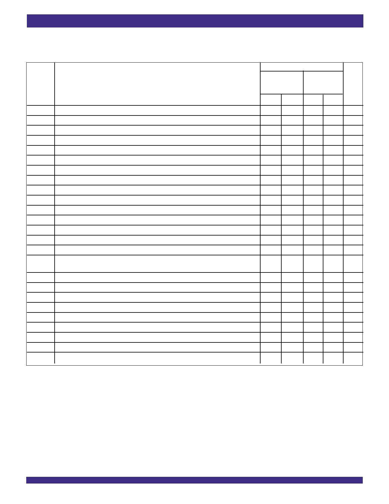
IDT723624/723634/723644 CMOS SyncBiFIFO™ WITH BUS-MATCHING
256 x 36 x 2, 512 x 36 x 2, 1,024 x 36 x 2
COMMERCIAL TEMPERATURE RANGE
TIMING REQUIREMENTS OVER RECOMMENDED RANGES OF SUPPLY
VOLTAGE AND OPERATING FREE-AIR TEMPERATURE
(Commercial: VCC = 5V ± 10%, TA = 0°C to +70°C)
Commercial
IDT723624L15
IDT723634L15
IDT723644L15
Symbol
Parameter
Min.
Max.
fS
Clock Frequency, CLKA or CLKB
—
66.7
tCLK
Clock Cycle Time, CLKA or CLKB
15
—
tCLKH Pulse Duration, CLKA or CLKB HIGH
6
—
tCLKL Pulse Duration, CLKA and CLKB LOW
6
—
tDS
Setup Time, A0-A35 before CLKA↑ and B0-B35 before CLKB↑
4
—
tENS1 Setup Time, CSA and W/RA before CLKA↑; CSB and W/RB before CLKB↑
4.5
—
tENS2 Setup Time ENA and MBA before CLKA↑; ENB and MBB before CLKB↑
4.5
—
tRSTS Setup Time, MRS1, MRS2, PRS1, or PRS2 LOW before CLKA↑ or CLKB↑(1)
5
—
tFSS
Setup Time, FS0 and FS1 before MRS1 and MRS2 HIGH
7.5
—
tBES
Setup Time, BE/FWFT before MRS1 and MRS2 HIGH
7.5
—
tSPMS Setup Time, SPM before MRS1 and MRS2 HIGH
7.5
—
tSDS
Setup Time, FS0/SD before CLKA↑
4
—
tSENS Setup Time, FS1/SEN before CLKA↑
4
—
tFWS
Setup Time, BE/FWFT before CLKA↑
0
—
tDH
Hold Time, A0-A35 after CLKA↑ and B0-B35 after CLKB↑
1
—
tENH
Hold Time, CSA, W/RA, ENA, and MBA after CLKA↑; CSB, W/RB, ENB, and MBB after CLKB↑
1
—
tRSTH Hold Time, MRS1, MRS2, PRS1 or PRS2 LOW after CLKA↑ or CLKB↑(1)
4
—
tFSH
Hold Time, FS0 and FS1 after MRS1 and MRS2 HIGH
2
—
tBEH
Hold Time, BE/FWFT after MRS1 and MRS2 HIGH
2
—
tSPMH Hold Time, SPM after MRS1 and MRS2 HIGH
2
—
tSDH
Hold Time, FS0/SD after CLKA↑
1
—
tSENH Hold Time, FS1/SEN HIGH after CLKA↑
1
—
tSPH
Hold Time, FS1/SEN HIGH after MRS1 and MRS2 HIGH
2
—
tSKEW1(2) Skew Time between CLKA↑ and CLKB↑ for EFA/ORA, EFB/ORB, FFA/IRA, and FFB/IRB
7.5
—
tSKEW2(2,3) Skew Time between CLKA↑ and CLKB↑ for AEA, AEB, AFA, and AFB
12
—
NOTES:
1. Requirement to count the clock edge as one of at least four needed to reset a FIFO.
2. Skew time is not a timing constraint for proper device operation and is only included to illustrate the timing relationship between CLKA cycle and CLKB cycle.
3. Design simulated, not tested.
Unit
MHz
ns
ns
ns
ns
ns
ns
ns
ns
ns
ns
ns
ns
ns
ns
ns
ns
ns
ns
ns
ns
ns
ns
ns
ns
8
Share Link: