IDT723624(2014) Просмотр технического описания (PDF) - Integrated Device Technology
Номер в каталоге
Компоненты Описание
Список матч
IDT723624
(Rev.:2014)
(Rev.:2014)
Integrated Device Technology

IDT723624 Datasheet PDF : 35 Pages
| |||
IDT723624/723634/723644 CMOS SyncBiFIFO™ WITH BUS-MATCHING
256 x 36 x 2, 512 x 36 x 2, 1,024 x 36 x 2
COMMERCIAL TEMPERATURE RANGE
DESCRIPTION:
The IDT723624/723634/723644 is a monolithic, high-speed, low-
power, CMOS bidirectional synchronous (clocked) FIFO memory which
supports clock frequencies up to 67 MHz and has read access times as fast as
10 ns. Two independent 256/512/1,024 x 36 dual-port SRAM FIFOs on board
each chip buffer data in opposite directions. FIFO data on Port B can be input
and output in 36-bit, 18-bit, or 9-bit formats with a choice of Big- or Little-Endian
configurations.
These devices are a synchronous (clocked) FIFO, meaning each port
employs a synchronous interface. All data transfers through a port are gated
to the LOW-to-HIGH transition of a port clock by enable signals. The clocks for
each port are independent of one another and can be asynchronous or
coincident. The enables for each port are arranged to provide a simple
bidirectional interface between microprocessors and/or buses with syn-
chronous control.
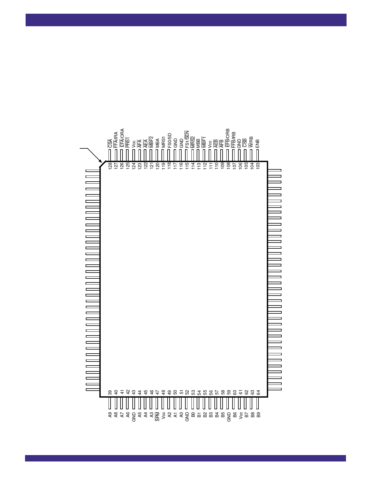
PIN CONFIGURATION
INDEX
W/RA
1
ENA
2
CLKA
3
GND
4
A35
5
A34
6
A33
7
A32
8
Vcc
9
A31
10
A30
11
GND
12
A29
13
A28
14
A27
15
A26
16
A25
17
A24
18
A23
19
BE/FWFT
20
GND
21
A22
22
Vcc
23
A21
24
A20
25
A19
26
A18
27
GND
28
A17
29
A16
30
A15
31
A14
32
A13
33
Vcc
34
A12
35
GND
36
A11
37
A10
38
TQFP (PK128-1, order code: PF)
TOP VIEW
2
102
CLKB
101
PRS2
100
Vcc
99
B35
98
B34
97
B33
96
B32
95
GND
94
GND
93
B31
92
B30
91
B29
90
B28
89
B27
88
B26
87
Vcc
86
B25
85
B24
84
BM
83
GND
82
B23
81
B22
80
B21
79
B20
78
B19
77
B18
76
GND
75
B17
74
B16
73
SIZE
72
Vcc
71
B15
70
B14
69
B13
68
B12
67
GND
66
B11
65
B10
3270 drw02
Share Link: