IDT723624(2014) Просмотр технического описания (PDF) - Integrated Device Technology
Номер в каталоге
Компоненты Описание
Список матч
IDT723624
(Rev.:2014)
(Rev.:2014)
Integrated Device Technology

IDT723624 Datasheet PDF : 35 Pages
| |||
IDT723624/723634/723644 CMOS SyncBiFIFO™ WITH BUS-MATCHING
256 x 36 x 2, 512 x 36 x 2, 1,024 x 36 x 2
COMMERCIAL TEMPERATURE RANGE
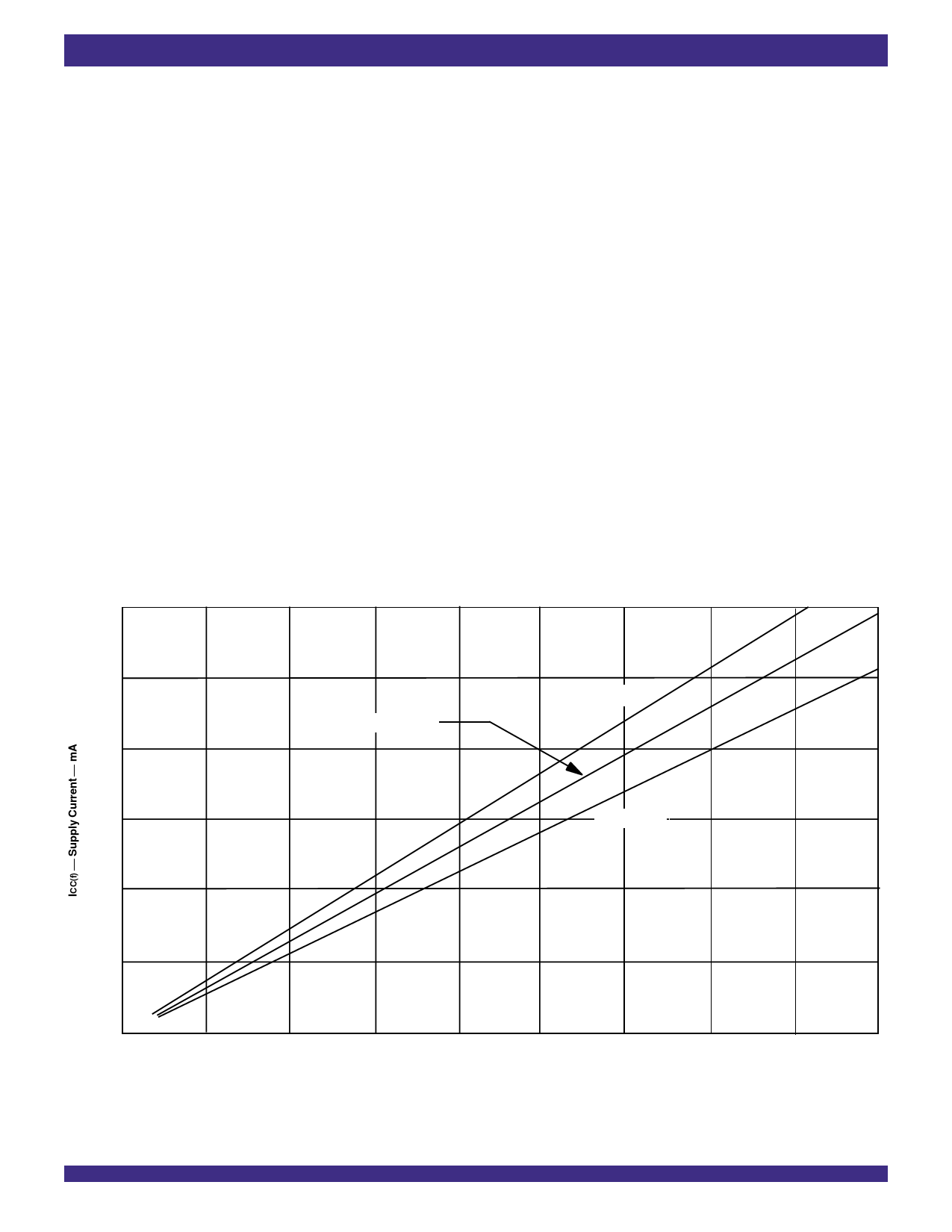
DETERMINING ACTIVE CURRENT CONSUMPTION AND POWER DISSIPATION
The ICC(f) current for the graph in Figure 1 was taken while simultaneously reading and writing a FIFO on the IDT723624/723634/723644 with
CLKA and CLKB set to fS. All data inputs and data outputs change state during each clock cycle to consume the highest supply current. Data
outputs were disconnected to normalize the graph to a zero capacitance load. Once the capacitance load per data-output channel and the number
of IDT723624/723634/723644 inputs driven by TTL HIGH levels are known, the power dissipation can be calculated with the equation below.
CALCULATING POWER DISSIPATION
With ICC(f) taken from Figure 1, the maximum power dissipation (PT) of these FIFOs may be calculated by:
PT = VCC x [ICC(f) + (N x ΔICC x dc)] + Σ(CL x VCC2 X fo)
where:
N
=
ΔICC =
dc
=
CL
=
fo
=
number of used outputs = 36-bit (long word), 18-bit (word) or 9-bit (byte) bus size
increase in power supply current for each input at a TTL HIGH level
duty cycle of inputs at a TTL HIGH level of 3.4 V
output capacitance load
switching frequency of an output
300
250
200
150
100
fdata = 1/2 fS
TA = 25°C
CL = 0pF
VCC = 5.0V
VCC = 5.5V
VCC = 4.5V
50
0
0
10
20
30
40
50
60
70
fS ⎯ Clock Frequency ⎯ MHz
Figure 1. Typical Characteristics: Supply Current (ICC) vs. Clock Frequency (fS)
7
80
90
3270 drw03
Share Link: