ICS663 Просмотр технического описания (PDF) - Integrated Device Technology
Номер в каталоге
Компоненты Описание
Список матч
ICS663 Datasheet PDF : 8 Pages
| |||
ICS663
PLL BUILDING BLOCK
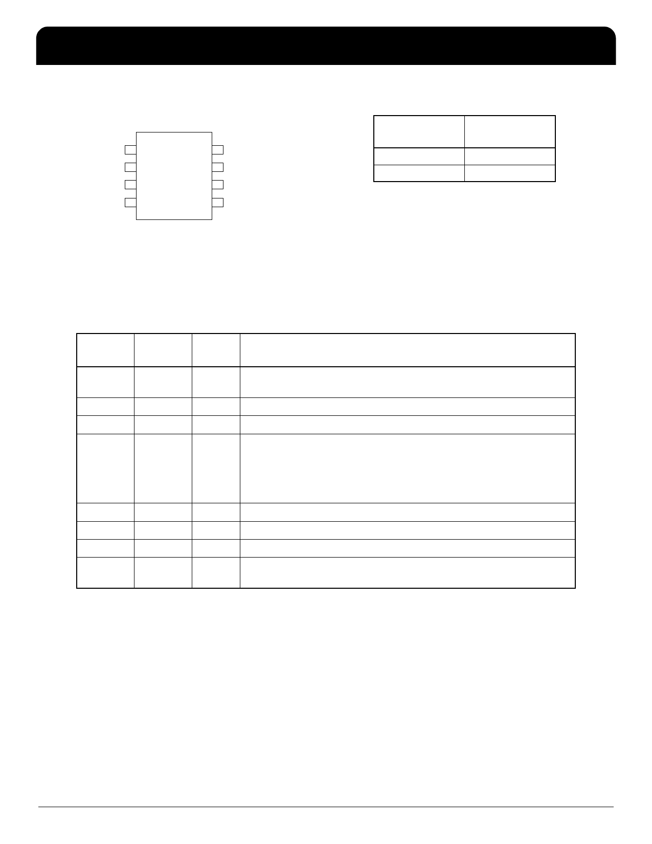
Pin Assignment
FBIN 1
VDD 2
GND 3
LF 4
8 REFIN
7 CLK
6 SEL
5 LFR
8 Pin (150 mil) SOIC
PLL BUILDING BLOCK
VCO Post Divide Select Table
SEL
VCO Post
Divide
0
8
1
2
0 = connect pin directly to ground
1 = connect pin directly to VDD
Pin Descriptions
Pin
Number
1
2
3
4
5
6
7
8
Pin
Name
FBIN
VDD
GND
LF
LFR
SEL
CLK
REFIN
Pin
Type
Pin Description
Input Feedback clock input. Connect the output of the feedback divider to
this pin. Falling edge triggered.
Power VDD. Connect to +3.3 V or +5 V.
Power Connect to ground.
Input
Loop filter connection (refer to Figure 1 on Page 5).
When using the phase detector block only, this pin serves as the
charge pump output.
When using the VCO block only, this pin serves as VCO input control
voltage.
Input Loop filter return (refer to Figure 1 on Page 5).
Input Select pin for VCO post divide, as per above table.
Output Clock output.
Input Reference clock input. Connect the input clock to this pin. Falling edge
triggered.
IDT™ / ICS™ PLL BUILDING BLOCK
2
ICS663
REV E 012006
Share Link: 