ICS663 Просмотр технического описания (PDF) - Integrated Device Technology
Номер в каталоге
Компоненты Описание
Список матч
ICS663 Datasheet PDF : 8 Pages
| |||
PLL BUILDING BLOCK
DATASHEET
ICS663
Description
The ICS663 is a low cost Phase-Locked Loop (PLL)
designed for clock synthesis and synchronization. Included
on the chip are the phase detector, charge pump, Voltage
Controlled Oscillator (VCO) and an output buffer. Through
the use of external reference and VCO dividers
(implemented with the ICS674-01, for example), the user
can easily configure the device to lock to a wide variety of
input frequencies.
The phase detector and VCO functions of the device can
also be used independently. This enables the configuration
of other PLL circuits. For example, the ICS663 phase
detector can be used to control a VCXO circuit such as the
MK3754.
For applications requiring Power Down or Output Enable
features, please refer to the ICS673-01.
Features
• Packaged in 8-pin SOIC (Pb free)
• Output clock range 1 MHz to 100 MHz (3.3 V), 1 MHz to
120 MHz (5 V)
• External PLL loop filter enables configuration for a wide
range of input frequencies
• Ability to accept an input clock in the kHz range (video
Hsync, for example)
• 25 mA output drive capability at TTL levels
• Lower power CMOS process
• +3.3 V ±5% or +5 V ±10% operating voltage
• Used along with the ICS674-01, forms a complete PLL
circuit
• Phase detector and VCO blocks can be used
independently for other PLL configurations
• Industrial temperature version available
• For better jitter performance, use the MK1575
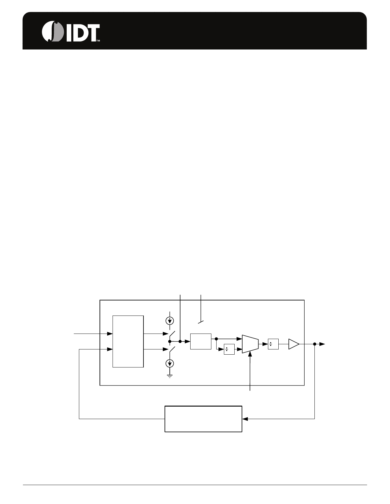
Block Diagram
Clock Input
R E F IN
F B IN
LF
LFR
VDD
Phase/
Frequency
Detector
Icp
UP
DOWN
VCO
Icp
1
MUX
2
4
0
CLK
SEL
External Feedback Divider
(such as the ICS674-01)
IDT™ / ICS™ PLL BUILDING BLOCK
1
ICS663
REV E 012006
Share Link: 