P4C163-25CM Просмотр технического описания (PDF) - Performance Semiconductor
Номер в каталоге
Компоненты Описание
Список матч
P4C163-25CM Datasheet PDF : 8 Pages
| |||
P4C163/P4C163L
ULTRA HIGH SPEED 8K x 9
STATIC CMOS RAMS
P4C163/163L
FEATURES
Full CMOS, 6T Cell
High Speed (Equal Access and Cycle Times)
– 25/35ns (Commercial)
– 25/35/45ns (Military)
Low Power Operation (Commercial/Military)
– 690/800 mW Active – 25
– 193/220 mW Standby (TTL Input)
– 5.5 mW Standby (CMOS Input) P4C163L
Output Enable and Dual Chip Enable Control
Functions
Single 5V±10% Power Supply
Data Retention with 2.0V Supply, 10 µA Typical
Current (P4C163L Military)
Common I/O
Fully TTL Compatible Inputs and Outputs
Standard Pinout (JEDEC Approved)
– 28-Pin 300 mil DIP, SOJ
– 28-Pin 350 x 550 mil LCC
– 28-Pin CERPACK
DESCRIPTION
The P4C163 and P4C163L are 73,728-bit ultra high-speed
static RAMs organized as 8K x 9. The CMOS memories re-
quire no clocks or refreshing and have equal access and
cycle times. Inputs are fully TTL-compatible. The RAMs op-
erate from a single 5V±10% tolerance power supply. With
battery backup, data integrity is maintained for supply volt-
ages down to 2.0V. Current drain is 10 µA from a 2.0V supply.
Access times as fast as 25 nanoseconds are available, per-
mitting greatly enhanced system operating speeds. CMOS
is used to reduce power consumption in both active and
standby modes.
The P4C163 and P4C163L are available in 28-pin 300 mil
DIP and SOJ and 28-pin 350 x 550 mil LCC packages provid-
ing excellent board level densities.
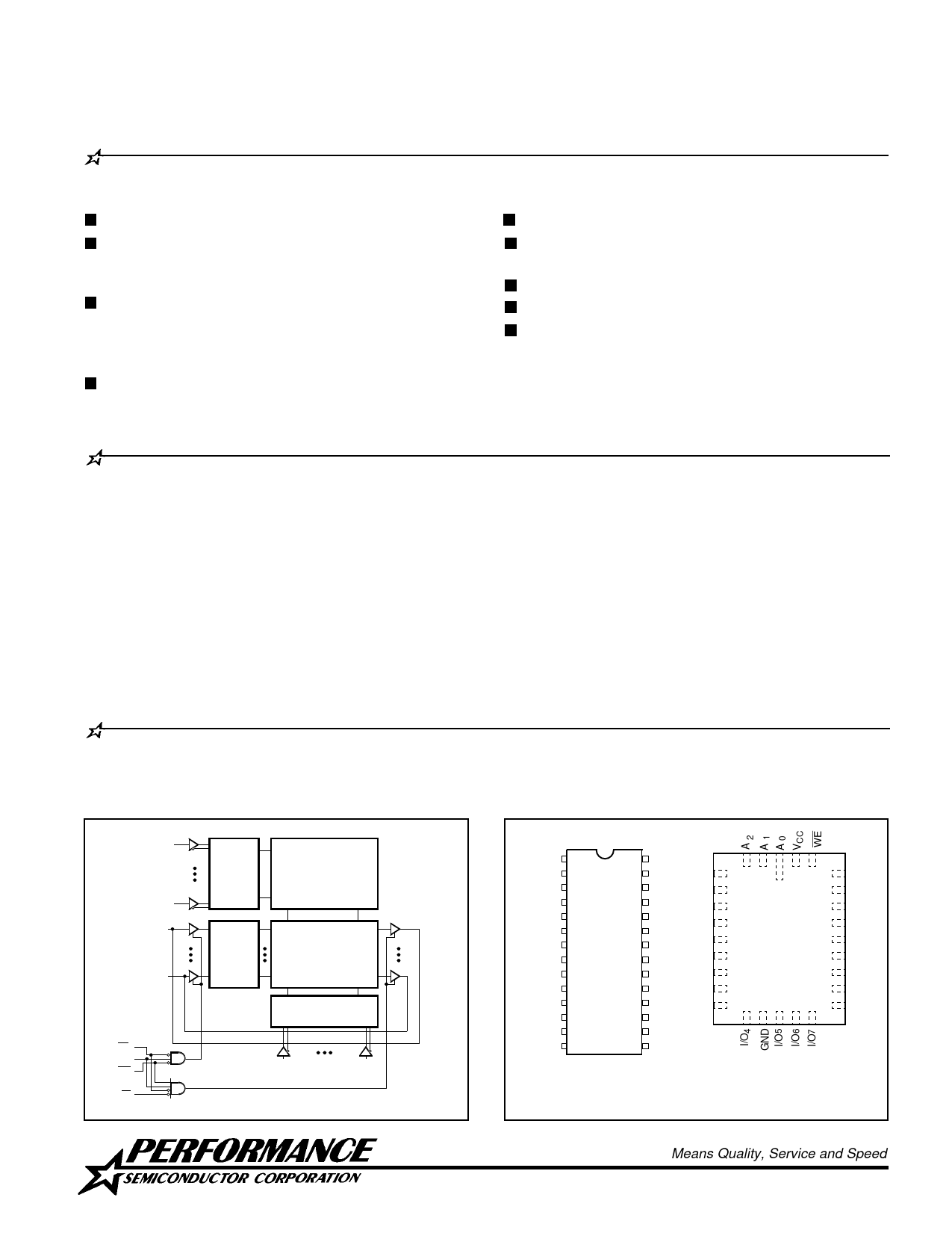
FUNCTIONAL BLOCK DIAGRAM
A0
A7
I/O 1
I/O 9
CE1
CE2
WE
OE
ROW
SELECT
73,728-BIT
MEMORY
ARRAY
INPUT
DATA
CONTROL
COLUMN I/O
COLUMN
SELECT
A8
A12
PIN CONFIGURATIONS
A0 1
A1 2
A2 3
A3 4
A4 5
A5 6
A6 7
A7 8
A8 9
I/O1 10
I/O2 11
I/O3 12
I/O4 13
GND 14
28 VCC
27 WE
A3
26 CE 2
A4
25 A12
A5
24 A 11
23 A10
22 OE
A6
A7
21 A 9
A8
20 CE1 I/O1
19 I/O 9 I/O 2
18 I/O 8 I/O 3
17 I/O 7
16 I/O 6
15 I/O 5
DIP (P5, C5), SOJ (J5)
CERPACK (F4) SIMILAR
TOP VIEW
3
27
4 2 28 26 CE2
5
1
25
A 12
6
24
A 11
7
23
A 10
8
22 OE
9
21 A 9
10
20
CE1
11
19 I/O9
12 14 15 16 18
I/O8
13
17
LCC (L5)
TOP VIEW
Means Quality, Service and Speed
1Q97
109
Share Link: 