74HC3G34 Просмотр технического описания (PDF) - Philips Electronics
Номер в каталоге
Компоненты Описание
Список матч
74HC3G34 Datasheet PDF : 16 Pages
| |||
Philips Semiconductors
Triple buffer gate
Product specification
74HC3G34; 74HCT3G34
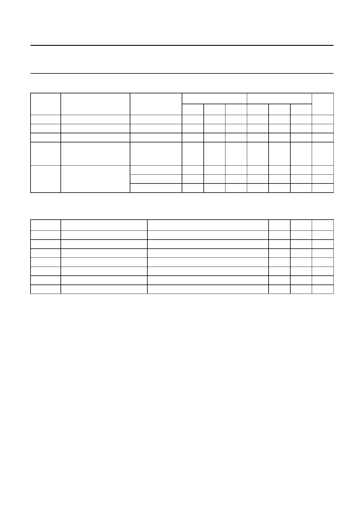
RECOMMENDED OPERATING CONDITIONS
SYMBOL
PARAMETER
VCC
VI
VO
Tamb
supply voltage
input voltage
output voltage
operating ambient
temperature
tr, tf
input rise and fall times
CONDITIONS
74HC3G34
74HCT3G34
UNIT
MIN. TYP. MAX. MIN. TYP. MAX.
2.0 5.0 6.0 4.5 5.0 5.5 V
0
−
VCC 0
−
VCC V
0
−
VCC 0
−
VCC V
see DC and AC −40 +25 +125 −40 +25 +125 °C
characteristics per
device
VCC = 2.0 V
VCC = 4.5 V
VCC = 6.0 V
−
−
1000 −
−
−
ns
−
6.0 500 −
6.0 500 ns
−
−
400 −
−
−
ns
LIMITING VALUES
In accordance with the Absolute Maximum Rating System (IEC 60134); voltages are referenced to GND (ground = 0 V).
SYMBOL
PARAMETER
VCC
supply voltage
IIK
input diode current
IOK
output diode current
IO
output source or sink current
ICC
VCC or GND current
Tstg
storage temperature
PD
power dissipation
CONDITIONS
VI < −0.5 V or VI > VCC + 0.5 V; note 1
VO < −0.5 V or VO > VCC + 0.5 V; note 1
−0.5 V < VO < VCC + 0.5 V; note 1
note 1
Tamb = −40 to +125 °C; note 2
MIN.
−0.5
−
−
−
−
−65
−
MAX. UNIT
+7.0 V
±20 mA
±20 mA
25
mA
50
mA
+150 °C
300 mW
Notes
1. The input and output voltage ratings may be exceeded if the input and output current ratings are observed.
2. Above 55 °C the value of PD derates linearly with 2.5 mW/K.
2003 May 19
5
Share Link: 