GD25Q20 Просмотр технического описания (PDF) - Unspecified
Номер в каталоге
Компоненты Описание
Список матч
GD25Q20 Datasheet PDF : 38 Pages
| |||
GD2UD5nuQiafol2ar0mnBdSxQeIcuGtaodxr SUenriiafol Frmlasshector dual and quadGsDe2ri5aQl 4fl0aBsh/20B
4. DEVICE OPERATION
SPI Mode
Standard SPI
The GD25Q20B feature a serial peripheral interface on 4 signals bus: Serial Clock (SCLK), Chip Select (CS#),
Serial Data Input (SI) and Serial Data Output (SO). Both SPI bus mode 0 and 3 are supported. Input data is latched on the
rising edge of SCLK and data shifts out on the falling edge of SCLK.
Dual SPI
The GD25Q20B supports Dual SPI operation when using the “Dual Output Fast Read” and “Dual I/O Fast Read”
(3BH and BBH) commands. These commands allow data to be transferred to or from the device at two times the rate of the
standard SPI. When using the Dual SPI command the SI and SO pins become bidirectional I/O pins: IO0 and IO1.
Quad SPI
The GD25Q20B supports Quad SPI operation when using the “Quad Output Fast Read”,” Quad I/O Fast Read”,
“Quad I/O Word Fast Read” (6BH, EBH, E7H) commands. These commands allow data to be transferred to or from the
device at four times the rate of the standard SPI. When using the Quad SPI command the SI and SO pins become
bidirectional I/O pins: IO0 and IO1, and WP# and HOLD# pins become IO2 and IO3. Quad SPI commands require the
non-volatile Quad Enable bit (QE) in Status Register to be set.
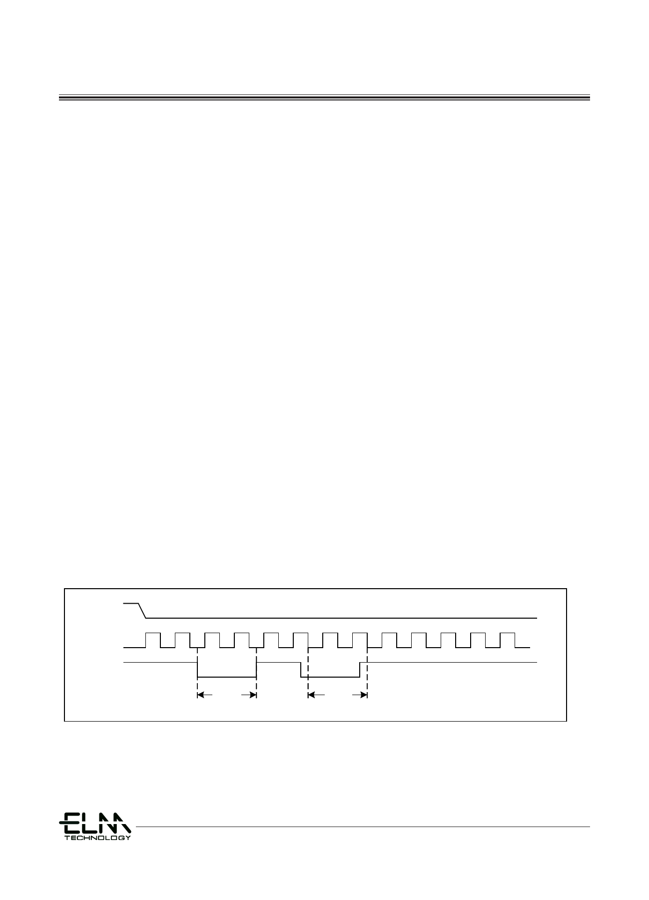
Hold
The HOLD# signal goes low to stop any serial communications with the device, but doesn’t stop the operation of write
status register, programming, or erasing in progress.
The operation of HOLD, need CS# keep low, and starts on falling edge of the HOLD# signal, with SCLK signal being
low (if SCLK is not being low, HOLD operation will not start until SCLK being low). The HOLD condition ends on rising edge
of HOLD# signal with SCLK being low (If SCLK is not being low, HOLD operation will not end until SCLK being low).
The SO is high impedance, both SI and SCLK don’t care during the HOLD operation, if CS# drives high during HOLD
operation, it will reset the internal logic of the device. To re-start communication with chip, the HOLD# must be at high and
then CS# must be at low.
Figure 1. Hold Condition
CS#
SCLK
HOLD#
HOLD
HOLD
9
38 - 8
Rev.1.1
Share Link: 