GD25Q20 Просмотр технического описания (PDF) - Unspecified
Номер в каталоге
Компоненты Описание
Список матч
GD25Q20 Datasheet PDF : 38 Pages
| |||
GD25UQni2fo0rBmxSIeGctxorUniform sector dual and quad serial flash
Dual and Quad Serial Flash
GD25Q40B/20B
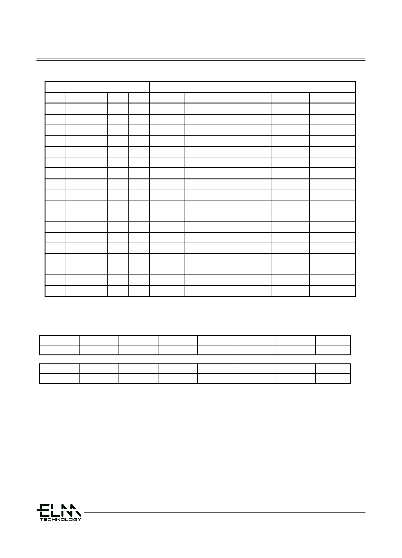
Table1a. GD25Q20B Protected area size (CMP=1)
Status Register Content
Memory Content
BP4 BP3 BP2 BP1 BP0
0
X
X
0
0
0
0
X
0
1
Blocks
0 to 3
0 to 2
Addresses
000000H-03FFFFH
000000H-02FFFFH
Density
256KB
192KB
Portion
ALL
Lower 3/4
0
0
X
1
0
0 and 1
000000H-01FFFFH
128KB
Lower 1/2
0
1
X
0
1
1 to 3
010000H-03FFFFH
192KB
Upper 3/4
0
1
X
1
0
2 and 3
020000H-03FFFFH
128KB
Upper 1/2
0
X
X
1
1
NONE
1
X
0
0
0
0 to 3
1
0
0
0
1
0 to 3
NONE
000000H-03FFFFH
000000H-03EFFFH
NONE
256KB
252KB
NONE
ALL
Lower 63/64
1
0
0
1
0
1
0
0
1
1
0 to 3
0 to 3
000000H-03DFFFH
000000H-03BFFFH
248KB
240KB
Lower 31/32
Lower 15/16
1
0
1
0
X
0 to 3
1
0
1
1
0
0 to 3
000000H-037FFFH
000000H-037FFFH
224KB
224KB
Lower 7/8
Lower 7/8
1
1
0
0
1
1
1
0
1
0
0 to 3
0 to 3
001000H-03FFFFH
002000H-03FFFFH
252KB
248KB
Upper 63/64
Upper 31/32
1
1
0
1
1
0 to 3
1
1
1
0
X
0 to 3
004000H-03FFFFH
008000H-03FFFFH
240KB
224KB
Upper 15/16
Upper 7/8
1
1
1
1
0
0 to 3
008000H-03FFFFH
224KB
Upper 7/8
1 X Un1 iform1 Sec1tor NONE
NONE
Dual and Quad Serial Flash
NONE
NONE
GD25Q40B/20B
6. STATUS REGISTER
S15
SUS
S14
CMP
S13
Reserved
S12
Reserved
S11
Reserved
S10
Reserved
S9
S8
QE
Reserved
S7
S6
S5
S4
S3
S2
S1
S0
SRP0
BP4
BP3
BP2
BP1
BP0
WEL
WIP
The status and control bits of the Status Register are as follows:
WIP bit.
The Write In Progress (WIP) bit indicates whether the memory is busy in program/erase/write status register progress.
When WIP bit sets to 1, means the device is busy in program/erase/write status register progress, when WIP bit sets 0,
means the device is not in program/erase/write status register progress.
WEL bit.
The Write Enable Latch (WEL) bit indicates the status of the internal Write Enable Latch. When set to 1 the internal
Write Enable Latch is set, when set to 0 the internal Write Enable Latch is reset and no Write Status Register, Program or
Erase command is accepted.
BP4, BP3, BP2, BP1, BP0 bits.
The Block Protect (BP4, BP3, BP2, BP1, BP0) bits are non-volatile. They define the size of the area to be software
protected against Program and Erase commands. These bits are written with the Write Status Register (WRSR) command.
When the Block
Table1).becomes
Protect (BP4, BP3, BP2, BP1,
protected against Page Program
BP0)
(PP),
bits are set
S3e8ct1o-3r 1E0rase
to 1, the relevant memory area (as
(SE) and Block Erase (BE) commands.
defineRd einv.1.1
The Block
Protect (BP4, BP3, BP2, BP1, BP0) bits can be written provided that the Hardware Protected mode has not been set. The
Chip Erase (CE) command is executed, if the Block Protect (BP4,BP3,BP2, BP1, BP0) bits are set to “None protected”.
SRP0 bit.
Share Link: 