T7264 Просмотр технического описания (PDF) - Agere -> LSI Corporation
Номер в каталоге
Компоненты Описание
Список матч
T7264 Datasheet PDF : 54 Pages
| |||
Data Sheet
April 1998
T7264 U-Interface 2B1Q Transceiver
Device Interface and Connections (continued)
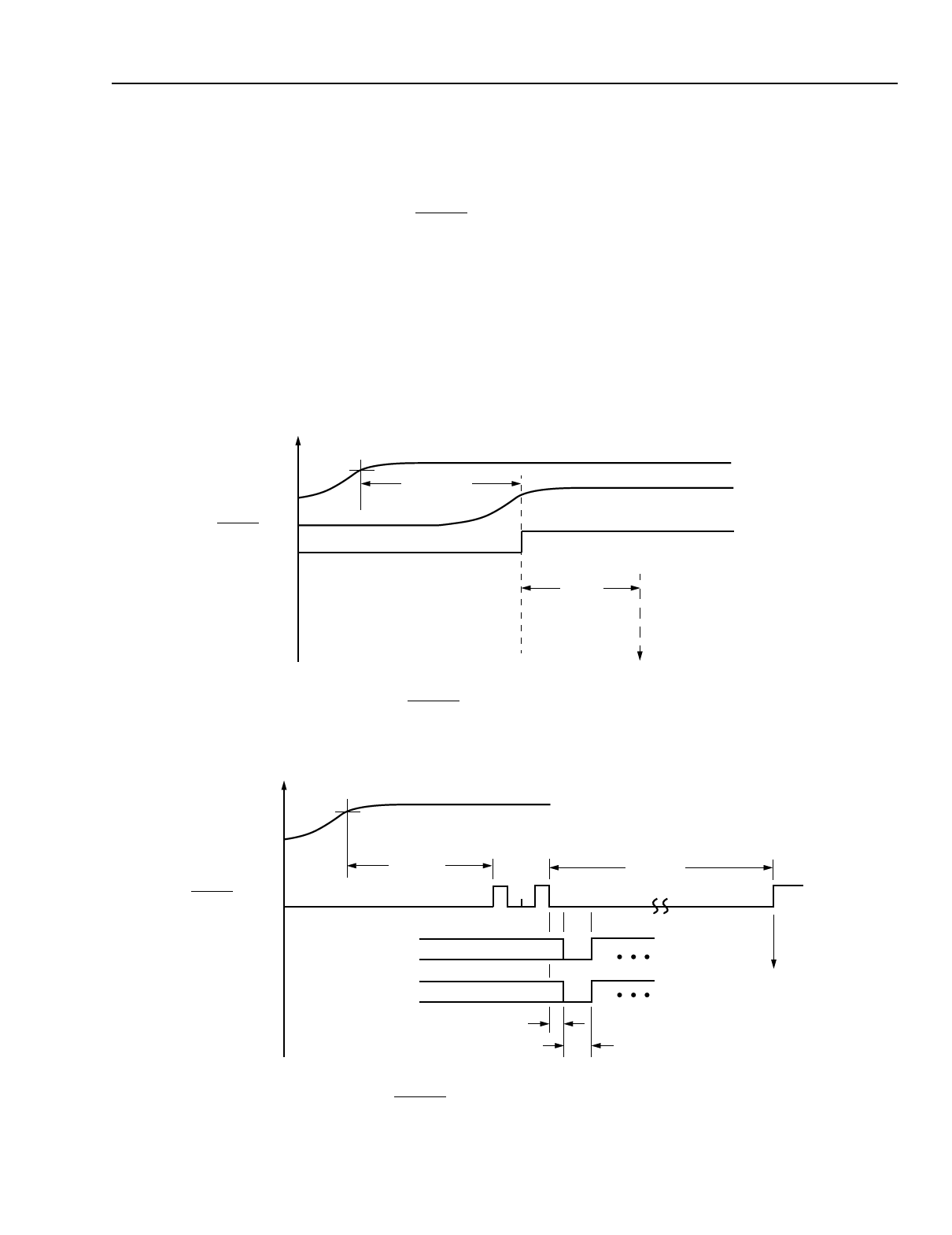
Reset Time
Reset time depends on the conditions under which the chip is reset. There are three cases to consider:
s When the chip is initially powered on, the RESET pin must be held low (below 0.5 V) for 1.5 ms. This allows
1.0 ms for the oscillator start-up and 0.5 ms for the digital reset process. An additional 1.0 ms is needed to allow
the analog circuitry to fully power up before the chip becomes fully functional.
s When the chip is in the idle mode, a software or hardware reset, applied for a minimum of three K2 frames, starts
the reset process. As before, the analog circuitry requires an additional 1.0 ms before the chip becomes fully
functional.
s If the chip is already fully powered up and functional, a software or hardware reset, applied for a minimum of
three K2 frames, is sufficient to complete the reset process.
When the chip is in the reset state, the output of the line driver is at 0 V and the transmit data is also 0 V.
POWER SUPPLY VOLTAGE
4.75 V
1.5 ms MIN
t
RESET PIN
INTERNAL RESET
(AFTER SCHMITT
TRIGGER)
t
1.0 ms
DEVICE REACHES POWER-ON
MODE (FULLY FUNCTIONAL)
Figure 6. RESET Waveform Normal Operation
5-5165a
4.75 V
RESET PIN
POWER SUPPLY VOLTAGE
≥2.5 ms
1 00 1
≥3 K2
FRAMES
F
UNDEFINED
C
UNDEFINED
1 MCLK PERIOD
NORMAL
RESET
AS IN FIGURE 6
2 MCLK PERIODS
5-5166a
Figure 7. RESET Timing for Synchronized Clocks
Lucent Technologies Inc.
9
Share Link: 