CDP1854 Просмотр технического описания (PDF) - Intersil
Номер в каталоге
Компоненты Описание
Список матч
CDP1854 Datasheet PDF : 21 Pages
| |||
CDP1854A, CDP1854AC
Absolute Maximum Ratings
DC Supply-Voltage Range, (VDD)
(Voltages Referenced to VSS Terminal)
CDP1854A . . . . . . . . . . . . . . . . . . . . . . . . . . . . . . . . .-0.5 to +11V
CDP1854AC . . . . . . . . . . . . . . . . . . . . . . . . . . . . . . . . .-0.5 to +7V
Input Voltage Range, All Inputs . . . . . . . . . . . . . .-0.5 to VDD + 0.5V
DC Input Current, Any One Input. . . . . . . . . . . . . . . . . . . . . . . . .±10mA
Device Dissipation Per Output Transistor
TA = Full Package-Temperature Range . . . . . . . . . . . . . . 100mW
Operating-Temperature Range (TA)
Package Type D . . . . . . . . . . . . . . . . . . . . . . . . . -55oC to +125oC
Package Type E and Q . . . . . . . . . . . . . . . . . . . . . -40oC to +85oC
Thermal Information
Thermal Resistance (Typical, Note 1)
θJA (oC/W) θJC (oC/W)
SBDIP Package . . . . . . . . . . . . . . . . . .
55
15
PDIP Package . . . . . . . . . . . . . . . . . . .
50
N/A
PLCC Package . . . . . . . . . . . . . . . . . .
46
N/A
Maximum Junction Temperature
Plastic Package . . . . . . . . . . . . . . . . . . . . . . . . . . . . . . . . . +150oC
Ceramic Package . . . . . . . . . . . . . . . . . . . . . . . . . . . . . . . +175oC
Maximum Storage Temperature Range (TSTG) . . .-65oC to +150oC
Maximum Lead Temperature (Soldering 10s):
At Distance 1/16 ±1/32 inch (1.59 ±0.79mm) . . . . . . . . . . +265oC
NOTE: Printed circuit board mount: 57mm x 57mm minimum area x
1.6mm thick G10 epoxy glass, or equivalent.
CAUTION: Stresses above those listed in “Absolute Maximum Ratings” may cause permanent damage to the device. This is a stress only rating and operation of
the device at these or any other conditions above those indicated in the operational sections of this specification is not implied.
NOTE:
1. θJA is measured with the component mounted on an evaluation PC board in free air.
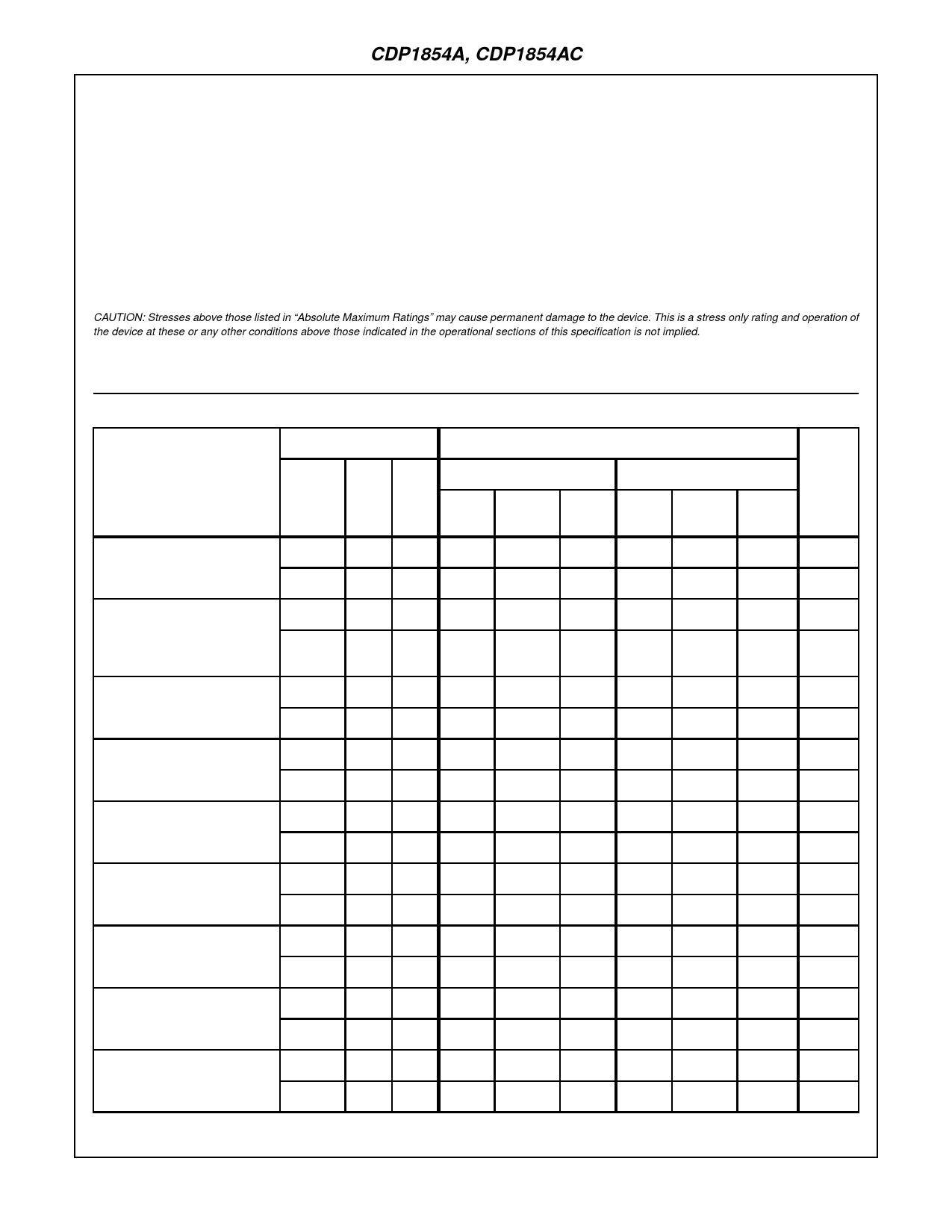
Static Electrical Specifications at TA = -40oC to +85oC, Unless Otherwise Noted
CONDITIONS
LIMITS
CDP1854A
CDP1854AC
PARAMETER
VO
VIN VDD
(NOTE 1)
(NOTE 1)
(V)
(V) (V) MIN
TYP
MAX MIN
TYP
MAX UNITS
Quiescent Device
IDD
-
0, 5
5
-
0.01
50
-
0.02
200
µA
Current
-
0, 10 10
-
1
200
-
-
-
µA
Output Low Drive
IOL
0.4
0, 5
5
1
2
(Sink) Current
(Except pins 24 and
0.5
0, 10 10
2
4
25)
-
1
2
-
-
-
-
mA
-
mA
Output High Drive
IOH
4.6
0, 5
5
-0.55
-1.1
-
-0.55
-1.1
-
mA
(Source) Current
9.5
0, 10 10
-1.3
-2.6
-
-
-
-
mA
Output Low Drive
(Sink) Current
(Pins 24 and 25)
IOL
0.4
0, 5
5
1.6
3.5
0.5
0, 10 10
3.2
7
-
1.6
3.5
-
-
-
-
mA
-
mA
Output Voltage
VOL
Low-Level (Note 2)
-
0, 5
5
-
-
0, 10 10
-
0
0.1
-
0
0.1
-
0
0.1
V
-
-
V
Output Voltage
VOH
-
0, 5
5
4.9
5
High-Level (Note 2)
-
0, 10 10
9.9
10
-
4.9
5
-
-
-
-
V
-
V
Input Low Voltage
VIL
0.5, 4.5
-
5
-
0.5, 9.5
-
10
-
-
1.5
-
-
3
-
-
1.5
V
-
-
V
Input High Voltage
VIH
0.5, 4.5
-
5
3.5
-
0.5, 9.5
-
10
7
-
-
3.5
-
-
-
-
-
V
-
V
Input Current
IIN
-
0, 5
5
-
-
0, 10 10
-
-
±1
-
-
±2
-
-
±1
µA
-
-
µA
5-45
Share Link: 