ISL6521 Просмотр технического описания (PDF) - Renesas Electronics
Номер в каталоге
Компоненты Описание
Список матч
ISL6521 Datasheet PDF : 14 Pages
| |||
ISL6521
1. The maximum rDS(ON) at the highest junction temperature.
2. The minimum IOCSET from the specification table.
3. Determine IPEAK for IPEAK > IOUT(MAX) + (I)/2, where I
is the output inductor ripple current.
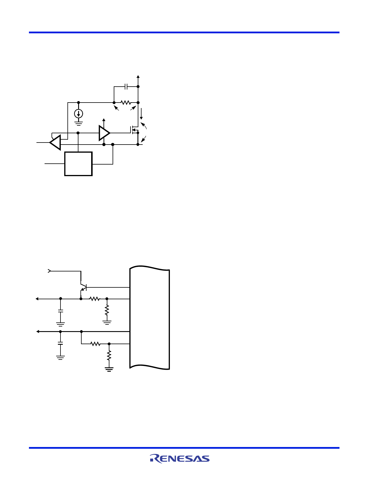
OVERCURRENT TRIP:
VDS > VSET
iD ¥ rDSON > IOCSET ¥ ROCSET
OCSET
VIN = +5V
ROCSET
OC
+
-
OCC
PWM
IOCSET
40A
DRIVE
GATE
CONTROL
VSET +
VCC
UGATE
PHASE
iD
+
VDS(ON)
VPHASE = VIN – VDS
VOCSET = VIN – VSET
FIGURE 3. OVERCURRENT DETECTION
For an equation for the ripple current see the section under
component guidelines titled ‘Output Inductor Selection’.
Output Voltage Selection
The output voltage of the PWM converter can be resistor-
programmed to any level between VIN and 0.8V. However,
since the value of RS1 is affecting the values of the rest of the
compensation components, it is advisable its value is kept
between 2k and 5k.
+5VIN
Q3
VOUT3
COUT3+
VOUT4
+
COUT4
DRIVE3
FB3
RS3
RP3
ISL6521
DRIVE4
FB4
RS4
RP4
in a parallel connection has to be less than 5k, or otherwise
said, the following relationship has to be met:
-RR----SS-----+-----RR-----PP- 5k
To ensure the parallel combination of the feedback resistors
equals a certain chosen value, RFB, use the following
equations:
RS = V---V--O--F--U--B--T-- RFB
RP = V----R-O----SU----T-----–-V----VF----BF----B- , where
VOUT - the desired output voltage,
VFB - feedback (reference) voltage, 0.8V.
Application Guidelines
Soft-Start Interval
The soft-start function controls the output voltages rate of rise to
limit the current surge at start-up. The soft-start function is
integrated on the chip and the soft-start interval is fixed.
PWM Controller Feedback Compensation
The PWM controller uses voltage-mode control for output
regulation. This section highlights the design consideration for
a PWM voltage-mode controller. Apply the methods and
considerations only to the PWM controller.
Figure 5 highlights the voltage-mode control loop for a
synchronous-rectified buck converter. The output voltage
(VOUT) is regulated to the reference voltage level, 0.8V. The
error amplifier (Error Amp) output (VE/A) is compared with the
oscillator (OSC) triangular wave to provide a pulse-width
modulated (PWM) wave with an amplitude of VIN at the
PHASE node. The PWM wave is smoothed by the output filter
(LO and CO).
The modulator transfer function is the small-signal transfer
function of VOUT/VE/A. This function is dominated by a DC
Gain, given by VIN/VOSC, and shaped by the output filter, with
a double pole break frequency at FLC and a zero at FESR.
VOUT
=
0.8
1
+
RR-----SP--
FIGURE 4. ADJUSTING THE OUTPUT VOLTAGE OF ANY OF
THE FOUR REGULATORS (OUTPUTS 3 AND 4
PICTURED)
Output voltage selection on the linear regulators is set by
means of external resistor dividers as shown in Figure 4. The
two resistors used to set the voltage on each of the three linear
regulators have to meet the following criteria: their value while
FN9148 Rev 2.00
Feb 8, 2005
Page 7 of 14
Share Link: 