ISL6521 Просмотр технического описания (PDF) - Renesas Electronics
Номер в каталоге
Компоненты Описание
Список матч
ISL6521 Datasheet PDF : 14 Pages
| |||
ISL6521
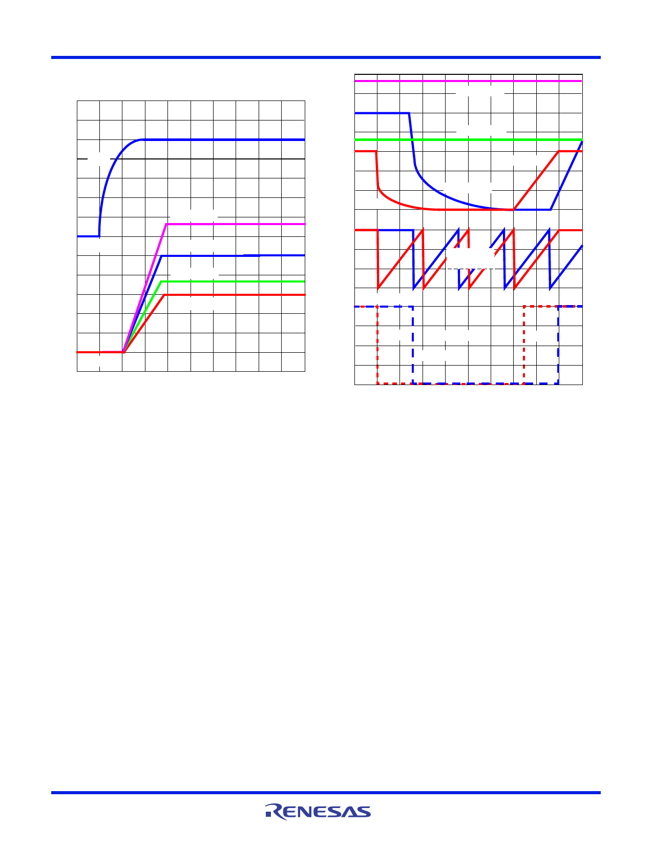
references of the linear controllers, ramp to their final value
bringing all outputs within regulation limits.
VOUT4 (3.3V)
+5V
0V
(1V/DIV)
VOUT4 (3.3V)
VOUT2 (2.5V)
VOUT3 (1.8V)
VOUT1 (1.5V)
(0.5V/DIV.)
0V
VOUT3 (1.8V)
VOUT1 (1.5V)
VOUT2 (2.5V)
SOFT-START
FUNCTION
UV MONITORING
0V
(0.5V/DIV)
T0 T1
T2
TIME
FIGURE 1. SOFT-START INTERVAL
Overcurrent Protection
All outputs are protected against excessive overcurrents. The
PWM controller uses the upper MOSFET’s on-resistance,
rDS(ON) to monitor the current for protection against a shorted
output. All linear controllers monitor their respective FB pins for
undervoltage events to protect against excessive currents.
A sustained overload (undervoltage on linears or overcurrent on
the PWM) on any output results in an independent shutdown of
the respective output, followed by subsequent individual re-start
attempts performed at an interval equivalent to 3 soft-start
intervals. Figure 2 describes the protection feature. At time T0,
an overcurrent event sensed across the switching regulator’s
upper MOSFET (rDS(ON) sensing) triggers a shutdown of the
VOUT1 output. As a result, its internal soft-start initiates a
number of soft-start cycles. After a three-cycle wait, the fourth
soft-start initiates a ramp-up attempt of the failed output, at time
T2, bringing the output in regulation at time T4.
To exemplify a UV event on one of the linears, at time T1, the
clock regulator (VOUT2) is also subjected to an overcurrent
event, resulting in a UV condition. Similarly, after three soft-
start periods, the fourth cycle initiates a ramp-up of this linear
output at time T3. One soft-start period after T3, the linear
output is within regulation limits. UV glitches less than 1s
(typically) in duration are ignored.
VOUT1
INACTIVE
VOUT2
ACTIVE
T0
T1
TIME
T2
T3 T4
FIGURE 2. OVERCURRENT/UNDERVOLTAGE PROTECTION
RESPONSE
Overcurrent protection is performed on the synchronous
switching regulator on a cycle-by-cycle basis. OC monitoring is
active as long as the regulator is operational. Since the
overcurrent protection on the linear regulators is performed
through undervoltage monitoring at the feedback pins (FB2,
FB3, and FB4), this feature is activated approximately 25%
into the soft-start interval (see Figure 2).
A resistor (ROCSET) programs the overcurrent trip level for
the PWM converter. As shown in Figure 3, the internal 40A
current sink (IOCSET) develops a voltage across ROCSET
(VSET) that is referenced to VIN . The DRIVE signal enables
the overcurrent comparator (OCC). When the voltage across
the upper MOSFET (VDS(ON)) exceeds VSET, the
overcurrent comparator trips to set the overcurrent latch. Both
VSET and VDS(ON) are referenced to VIN and a small
capacitor across ROCSET helps VOCSET track the variations
of VIN due to MOSFET switching. The overcurrent function
will trip at a peak inductor current (IPEAK) determined by:
IPEAK = I--O-----C----S----Er--D--T---S------OR----N-O----C-----S----E----T-
The OC trip point varies with MOSFET’s rDS(ON) temperature
variations. To avoid overcurrent tripping in the normal
operating load range, determine the ROCSET resistor from
the equation above with:
FN9148 Rev 2.00
Feb 8, 2005
Page 6 of 14
Share Link: 