6V62160E Просмотр технического описания (PDF) - LAPIS Semiconductor Co., Ltd.
Номер в каталоге
Компоненты Описание
Список матч
6V62160E Datasheet PDF : 33 Pages
| |||
FEDD56V62160E-07
MD56V62160E
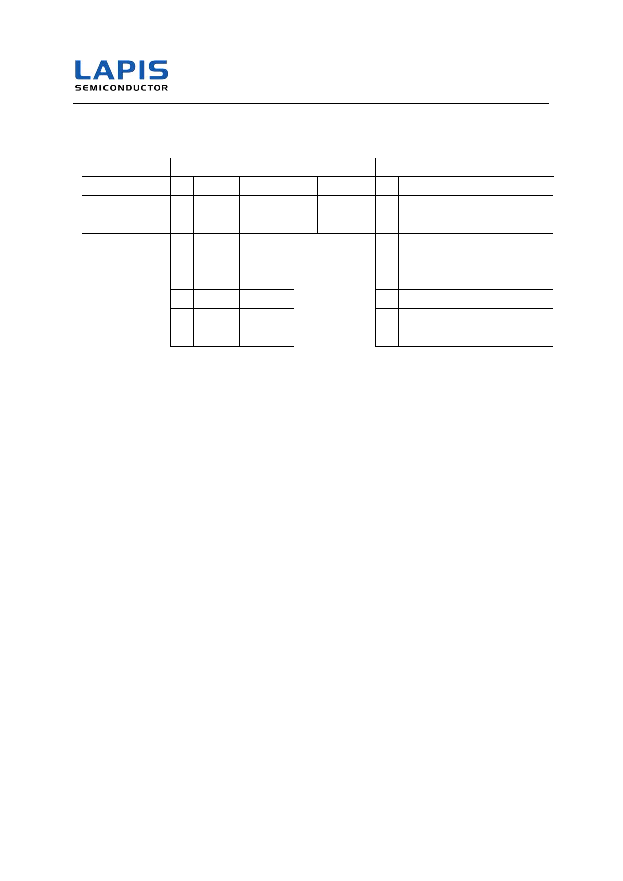
Mode Set Address Keys
Single Write
CAS Latency
Burst Type
Burst Length
A9 BRSW A6 A5 A4
CL
A3
BT
A2 A1 A0 BT = 0 BT = 1
0 Normal 0 0 0 Reserved 0 Sequential 0 0 0
1
1
1 Single Write 0 0 1 Reserved 1 Interleave 0 0 1
2
2
010
2
010
4
4
011
3
011
8
8
1 0 0 Reserved
1 0 0 Reserved Reserved
1 0 1 Reserved
1 0 1 Reserved Reserved
1 1 0 Reserved
1 1 0 Reserved Reserved
1 1 1 Reserved
1 1 1 Full Page Reserved
Notes: A7, A8, A10, A11, A12 and A13 should stay “L” during mode set cycle.
MD56V62160E supports two methods of Power on Sequence.
POWER ON SEQUENCE 1
1. With inputs in NOP state, turn on the power supply and start the system clock.
2. After the VCC voltage has reached the specified level, pause for 200 s or more with the input kept in
NOP state.
3. Issue the precharge all bank command.
4. Apply a CBR auto-refresh eight or more times.
5. Enter the mode register setting command.
POWER ON SEQUENCE 2
1. With inputs in NOP state, turn on the power supply and start the system clock.
2. After the VCC voltage has reached the specified level, pause for 200 s or more with the input kept in
NOP state.
3. Issue the precharge all bank command.
4. Enter the mode register setting command.
5. Apply a CBR auto-refresh eight or more times.
6/33
Share Link: 