RV5C386A_03 Просмотр технического описания (PDF) - RICOH Co.,Ltd.
Номер в каталоге
Компоненты Описание
Список матч
RV5C386A_03
RICOH Co.,Ltd.

RV5C386A_03 Datasheet PDF : 49 Pages
| |||
RV5C386A
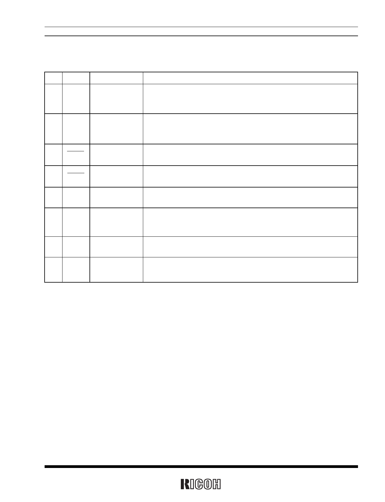
PIN DESCRIPTIONS
Pin No. Symbol
Item
2 SCL Serial clock line
Description
This pin is used to input shift clock pulses to synchronize data input/output to and
from the SDA pin with this clock. Allows a maximum input voltage of 5.5 volts
regardless of supply voltage.
3 SDA Serial data line
This pin inputs and outputs written or read data in synchronization with shift clock
pulses from the SCL pin. Allows a maximum input voltage of 5.5 volts regardless
of supply voltage.
This pin outputs periodic interrupt pulses and alarm interrupt (Alarm_D) to the
6 INTRA Interrupt output A
CPU. This pin is off when power is activated from 0V. Nch. open drain output.
This pin is used to output alarm interrupt signals(Alarm_W) to the CPU. This pin
4 INTRB Interrupt output B
is off when power is activated from 0V. Nch. open drain output.
The 32KOUT pin is used to output 32.768kHz clock pulses. CMOS push-pull
1 32KOUT 32-kHz Clock Output
output. The output is disabled if the CLKC pin is set to “L” or open.
The CLKC pin is used to control output of the 32KOUT pin. The clock output is
7 CLKC Clock Control Input disabled and held low when the pin is set to “L”or open. Incorporates a pull down
resistor.
9 OSCIN Oscillatory Circuit The OSCIN and OSCOUT pins are used to connect the 32.768-kHz crystal
8 OSCOUT Input/Output
oscillator (with all other oscillation circuit components built into the RV5C386A).
10 VDD Positive Power Supply Input
The VDD pin is connected to the power supply. The VSS pin is grounded.
5
VSS Negative Power Supply Input
3
Share Link: