ZR36050 Просмотр технического описания (PDF) - Zoran Corporation
Номер в каталоге
Компоненты Описание
Список матч
ZR36050 Datasheet PDF : 52 Pages
| |||
ADVANCE INFORMATION
ZR36050
Expansion (Full or Fast Preview)
s The ZR36050 reads compressed data from the Compressed
Data Interface or the Host Interface, as selected by the
HARDWARE register, into the Code Buffer.
Whenever it encounters a marker segment, it writes the seg-
ment in the appropriate location in Internal Memory, decodes
the information contained in the segment and sets the appro-
priate marker bit in the STATUS_0 register. If the correspond-
ing interrupt request is enabled, the ZR36050 stops
processing the compressed data, activates INT, and waits for
the host to restart processing by issuing the GO command.
If an APP (or COM) marker is encountered, and the length of
the segment is greater than 64 bytes, the host can read it out
by a method similar to that used in encoding, if the APP (or
COM) interrupt request is enabled. The ZR36050 writes 64
bytes at a time (or fewer in the last section) in the internal
memory, sets the APP (or COM) status bit, and waits for the
host to intervene and read the data. If the interrupt request
bit was not set, the ZR36050 writes the first 64 bytes of the
segment into internal memory and continues processing,
discarding the remainder of the segment.
s If the frame marker is SOF3, the ZR36050 switches to JPEG
Lossless decoding.
s The Zr36050 decodes the SOS marker segment, and
determines the number of blocks (JPEG Baseline) or
samples (JPEG Lossless) of each component of the scan (in
the MCU). The ZR36050 then sets the RFD status bit when
it has completed processing the markers and the Pixel
Interface is ready to send out the first image samples.
s The ZR36050 decodes the first scan of the compressed
image and outputs the expanded image samples via the
Pixel Interface. It outputs an EOS signal together with the last
sample of the scan, and sets the RFM status bit at the same
time.
s If there is more than one scan, the ZR36050 repeats the scan
decoding until all scans have been processed.
s The ZR36050 sets the END status bit, activates the END
signal, and goes to the Idle state.
Note: At the end of a decoding process, the ZR36050 performs
up to two extra read cycles. Therefore the system must allow the
ZR36050 to read up to two Compressed Data Memory bytes
after the EOI marker. These bytes may be any value, including
“FF”.
Tables Preload for Decoding
s The ZR36050 preloads the tables specified by the DQTI and
DHTI bits of the MARKERS_EN register. If DQTI is set, the
ZR36050 reads the quantization tables specified in the DQT
marker segment of the Internal Memory, multiples them by
the Scale Factor, and stores them in the Quantization Table
Store. If DHTI is set, the ZR36050 decodes the Huffman
tables specified in the DHT segment of the Internal Memory,
and stores the decoded tables in the Huffman Table Store.
s It sets the END status bit and activates the END signal, and
goes into the Idle state.
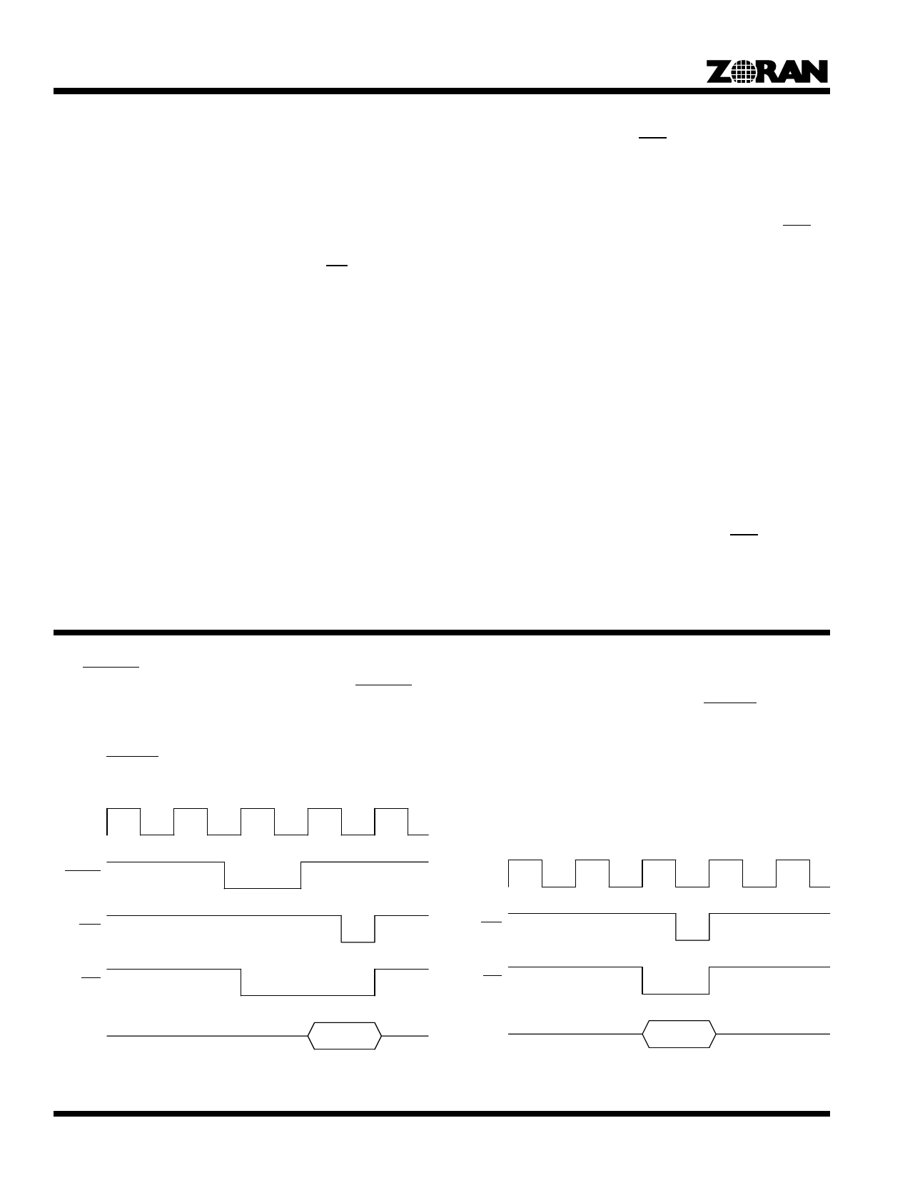
FREEZE OPERATION
The FREEZE signal freezes all ZR36050 operations. It is
sampled on the rising edge of CLK_IN. Once FREEZE is
sampled, all buses float immediately, and the activities of the
ZR36050 are frozen in their current state. The output control
signals that are activated on the same rising edge of CLK_IN that
samples FREEZE will be activated but frozen in their new states.
However, the activation of the control signals that become active
with 0.5 DCLK delay with respect to rising edge of CLK_IN (for
example, CRD, CWR) will be delayed until FREEZE is deactivat-
ed. Figures 6 and 7 show an example of Freeze and Normal
operation for compressed Data memory write cycle with
CFIS=01 (2 CLK_IN cycles).
CLK_IN
FREEZE
CLK_IN
CWE
CWE
CCS
CCS
CODE
Figure 6. Freeze Operation for Compressed Data Memory
Write Cycle with CFIS=01
CODE
Figure 7. Normal Operation for Compressed Data Memory
Write Cycle with CFIS=01
18
Share Link: 