A3G4250D Просмотр технического описания (PDF) - STMicroelectronics
Номер в каталоге
Компоненты Описание
Список матч
A3G4250D Datasheet PDF : 44 Pages
| |||
A3G4250D
4
Application hints
Application hints
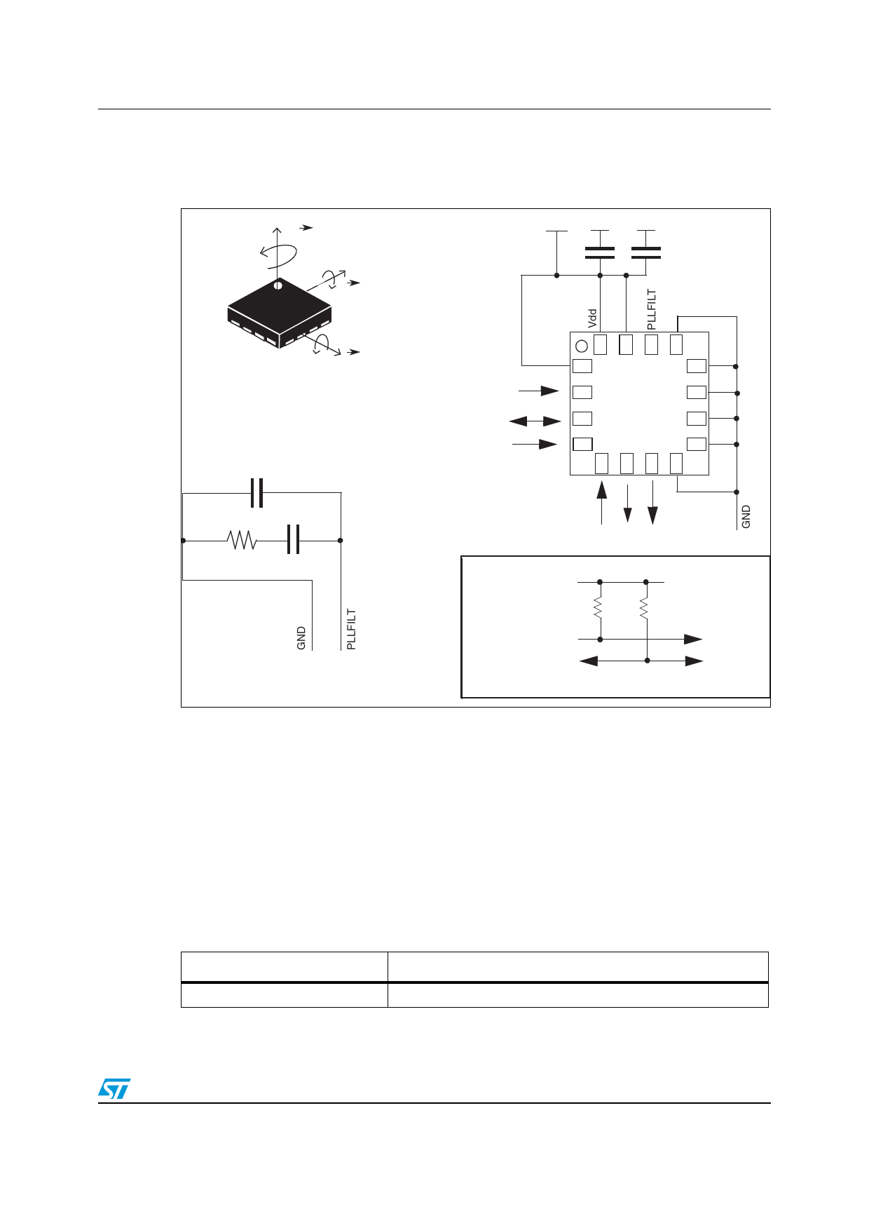
Figure 11. A3G4250D electrical connections and external component values
+ΩZ
Vdd GND GND
1
X
+ΩY
100 nF
10 µF
+ΩX
(TOP VIEW)
DIRECTIONS OF THE
DETECTABLE
ANGULAR RATES
10nF C1
Vdd_IO
SCL/SPC
SDA_SDI_SDO
SDO/SA0
16
13
1
12
TOP
VIEW
4
5
9
8
10kOhm
470nF
R2
C2
CS DR INT
Vdd I2C bus
Rpu Rpu = 10kOhm
AM07949V1
SCL/SPC
SDA_SDI_SDO
Pull-up to be added when I2C interface is used
Power supply decoupling capacitors (100 nF ceramic or polyester +10 µF) should be placed
as near as possible to the device (common design practice).
If Vdd and Vdd_IO are not connected together, power supply decoupling capacitors
(100 nF and 10 µF between Vdd and common ground, 100 nF between Vdd_IO and
common ground) should be placed as near as possible to the device (common design
practice).
The A3G4250D IC includes a PLL (phase locked loop) circuit to synchronize driving and
sensing interfaces. Capacitors and resistors must be added at the PLLFILT pin (as shown in
Figure 11) to implement a second-order low-pass filter. Table 10 summarizes the PLL low-
pass filter component values.
Table 10. PLL low-pass filter component values
Component
Value
C1
10 nF ± 10%
Doc 022768 Rev 3
21/44
Share Link: 