GF9101 Просмотр технического описания (PDF) - Gennum -> Semtech
Номер в каталоге
Компоненты Описание
Список матч
GF9101 Datasheet PDF : 23 Pages
| |||
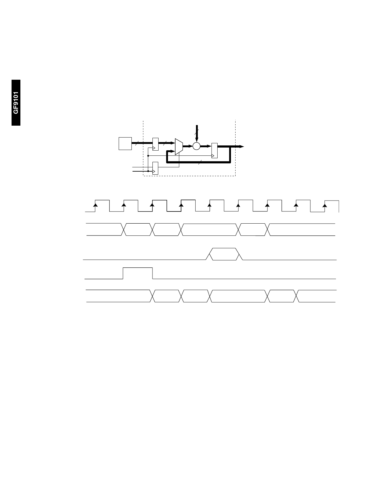
PIPELINE_IN, PIPELINE_OUT STAGE
The calculated filter sum from the adder tree and delay
enters into the pipelined output stage. Figure 5 shows the
block diagram for the pipelined structure. FB_SEL
determines whether the sum is added to the current
PIPELINE_OUT or the registered PIPELINE_IN. The result is
then registered at PIPELINE_OUT. When using one GF9101,
this configuration can be used to add two partial filter sums
from the A and B registers. Another application would be to
use the PIPELINE_IN port for adding DC offset or SYNC
and BURST signals (i.e. for 4:2:2 to 4ƒSC rate conversion).
This can be achieved by clocking in the SYNC and BURST
signals from an external PROM connected to the
PIPELINE_IN.
By connecting PIPELINE_OUT of one GF9101 device to
PIPELINE_IN of another, up to three GF9101’s may be
cascaded to form larger filters.
PIPELINE–IN
20
PROM
FB–SEL
CLK–IN
20
R
R
FILTER–SUM
20
0
+
1
R
20
GF9101
PIPELINE–OUT
Fig. 5 Block Diagram for Pipelined Output Stage
CLK_IN
FILTER_SUM
XXX
PIPELINE_IN
SUM 1
SUM 2
XXX
SUM 3
003H
XXX
FB_SEL
PIPELINE_OUT
XXX
SUM 1
SUM 1
+
SUM 2
XXX
Fig. 6 Timing Diagram for the Pipelined Output Stage
00+3H
SUM 3
XXX
APPLICATION NOTES
Video applications for the GF9101 include video rate
conversion and high performance FIR filters. The following
section presents a number of examples which show odd
and even symmetric and asymmetric filters.
ODD-TAP SYMMETRIC FILTER
The GF9101 can be configured as an Odd-tap symmetric
filter. A 23-tap odd-symmetric filter using one GF9101 will
be discussed. For an odd-tap symmetric filter, the
configuration word is shown in Table 7.
The maximum data rate using this filter configuration is 20
MHz, where the filter is clocked at twice the data rate of 40
MHz, the frequency of CLK_IN. The filter has input data An
and filter data coefficients Cn (C0 —> C11) as shown in
Figure 7. The input enters the filter at DATA_A_IN and exits
the filter from DATA_B_OUT. The coefficient C11 is only
multiplied by the data in reg. A_12 and reg.B_12 is
bypassed. The data is shifted into the register by clocking
ENA and ENB at the same time at half the CLK_IN
frequency. The filter timing is shown in Figure 8.
8
520 - 64 - 7
Share Link: 