GF9101 Просмотр технического описания (PDF) - Gennum -> Semtech
Номер в каталоге
Компоненты Описание
Список матч
GF9101 Datasheet PDF : 23 Pages
| |||
need to be loaded into the internal RAM. If location 0 is
used for filtering, MB0 > MB5 must be loaded for this
location. The example shown in Figure 2 loads the value
BBH into TEMP_REG_A.
LOAD_EN
COEF-WR
COEF_DATA
(7-0)
BBH
COEF_ADDR
(9-0)
300H
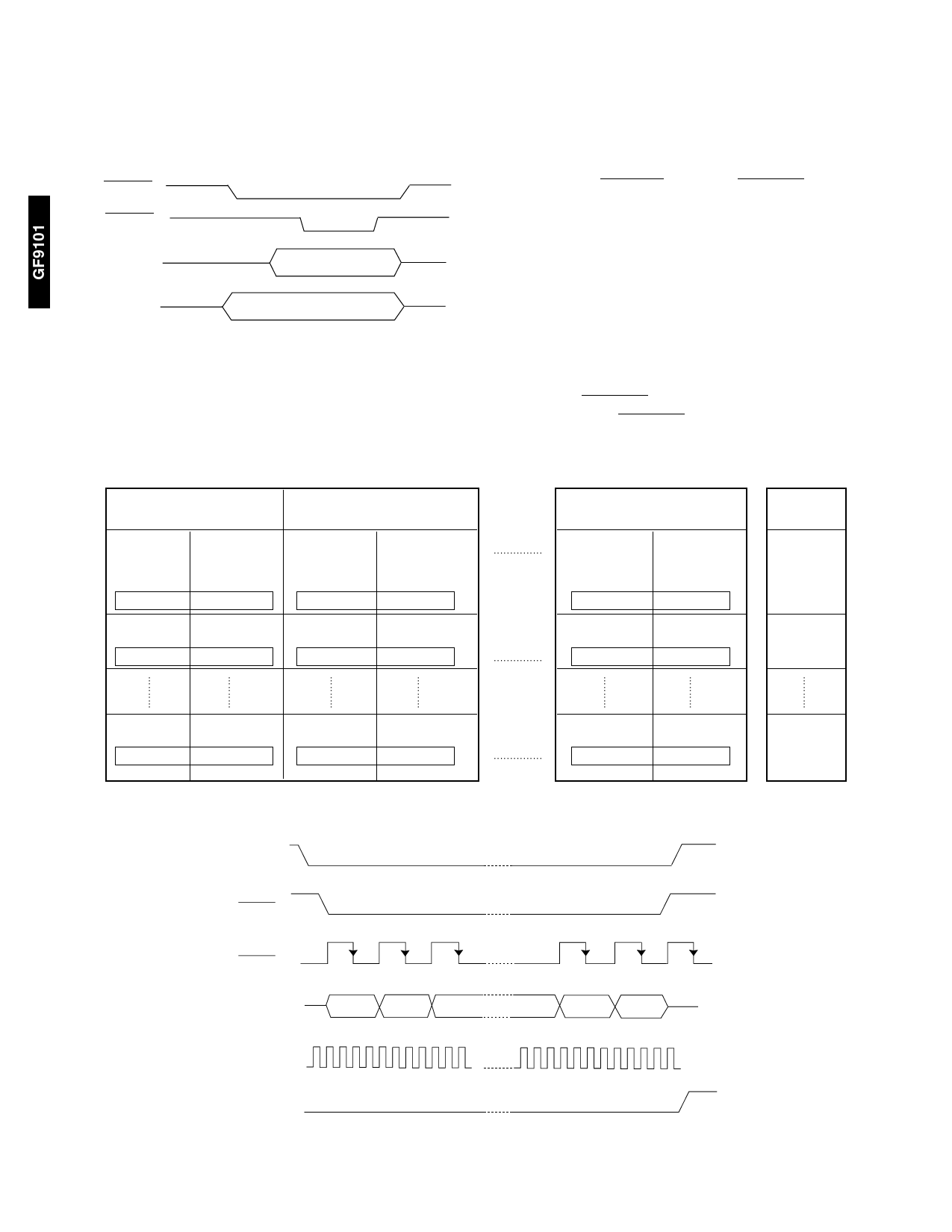
Fig. 2 Microprocessor Loading Timing Diagram
TABLE 6: Serial Mode Loading Order
Memory Bank 0
Memory Bank 1
TAP 2
TAP 1
1,2,3 .... 12 13 ........ 24
0,1,2 .... 11 0 .......... 11
25 .................................. 48
0 .......... 11 0 .......... 11
TAP4
TAP 3
2593 ............................. 2617
0 .......... 11 0 .......... 11
2618 ............................. 2642
0 .......... 11 0 .......... 11
SERIAL LOADING
Serial loading is sequential and synchronous. If serial
loading is selected the GF9101 will not enter the run mode
until the entire serial load sequence is completed at which
time the S_LOAD_CMP signal will go high. A bit will be
written each time LOAD_EN is low and COEF_WR makes a
high to low transition. Once the GF9101 is configured for
serial loading, 24 x 108 x 6 =15552 bits must be written
before the run mode is entered automatically. The 15552
bits must be entered in the order defined in Table 6. MB0 is
loaded first from RAM location 0 starting to fill the first 12
bits of tap 2. MB5 RAM location 107, tap 11 is loaded last.
When the serial load sequence is completed,
S_LOAD_CMP will go high and the run mode will be active.
Below is a serial loading timing diagram. This example
shows the serial loading start-up sequence. Notice that the
falling edge of COEF_WR is used to register the serial data.
The frequency of COEF_WR should be ≤1/4 CLK_IN
frequency.
Memory Bank 5
TAP12
TAP 11
5185 ............................. 5208
0 .......... 11 0 .......... 11
5209 ............................. 5233
0 .......... 11 0 .......... 11
Ram
Location
0
1
2568 ............................. 2592
0,1,2 .... 11 0 .......... 11
5160 ............................. 5184
0 .......... 11 0 .......... 11
15528 ...........................15552
0 .......... 11 0 .......... 11
107
520 - 64 - 7
CONFIGURE
LOAD_EN
COEF_WR
COEF_DATA (7)
BIT 1
BIT 2
BIT 3
BIT 15551 BIT 15552
CLK_IN
S_LOAD_CMP
Fig. 3 Serial Mode Timing Diagram
6
Share Link: 