PHB33NQ20T Просмотр технического описания (PDF) - NXP Semiconductors.
Номер в каталоге
Компоненты Описание
Список матч
PHB33NQ20T Datasheet PDF : 12 Pages
| |||
NXP Semiconductors
PHB33NQ20T
N-channel TrenchMOS standard level FET
2. Pinning information
Table 2. Pinning information
Pin
Symbol Description
1
G
gate
2
D
drain
3
S
source
mb
D
mounting base; connected to
drain
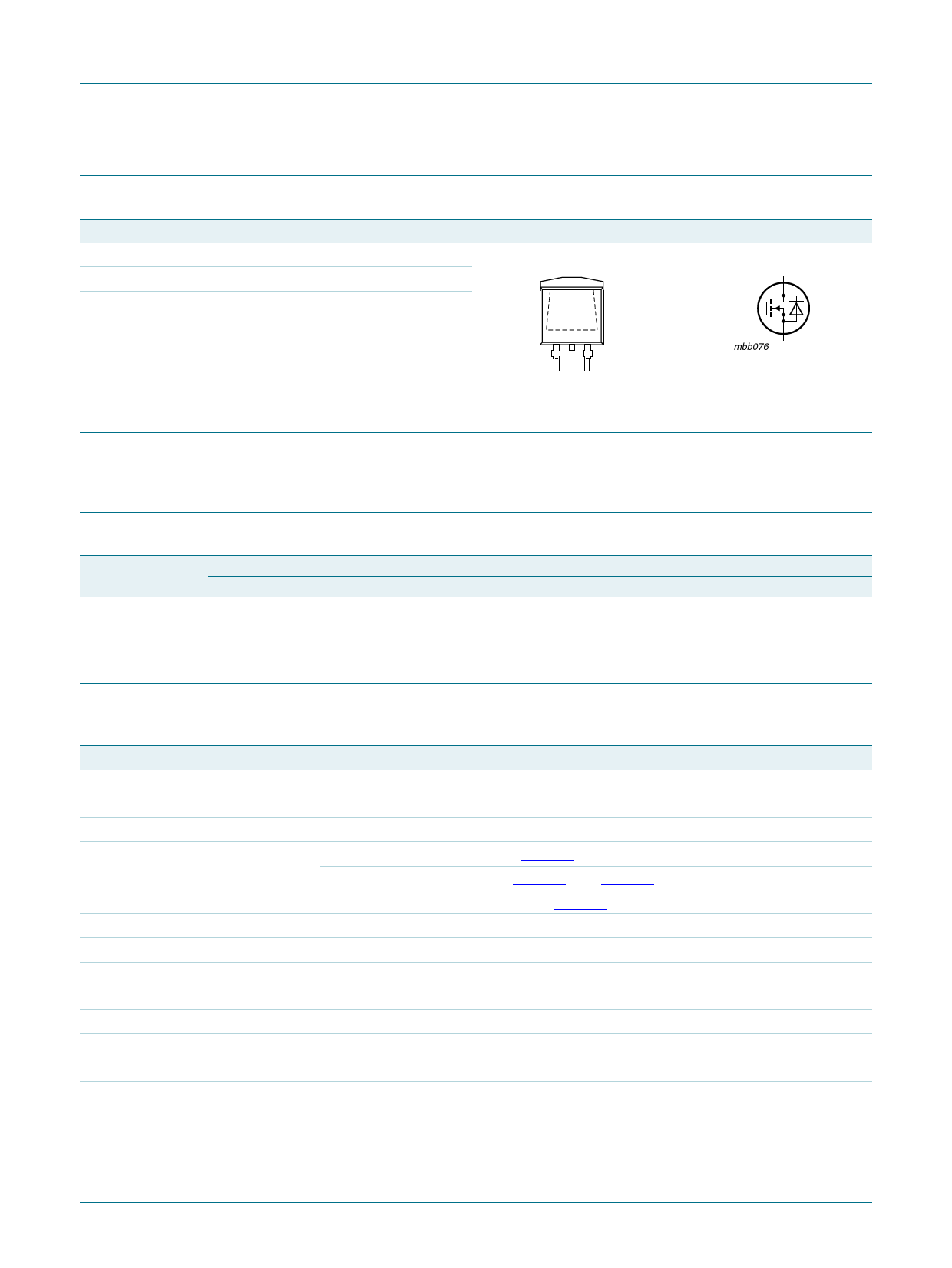
Simplified outline
mb
[1]
2
13
SOT404
(D2PAK)
[1] It is not possible to make a connection to pin 2.
3. Ordering information
Graphic symbol
D
G
mbb076 S
Table 3. Ordering information
Type number
Package
Name
Description
PHB33NQ20T D2PAK
plastic single-ended surface-mounted package (D2PAK); 3 leads (one
lead cropped)
Version
SOT404
4. Limiting values
Table 4. Limiting values
In accordance with the Absolute Maximum Rating System (IEC 60134).
Symbol Parameter
Conditions
VDS
VDGR
VGS
ID
drain-source voltage
drain-gate voltage
gate-source voltage
drain current
IDM
peak drain current
Ptot
total power dissipation
Tstg
storage temperature
Tj
junction temperature
Source-drain diode
Tj ≥ 25 °C; Tj ≤ 175 °C
Tj ≥ 25 °C; Tj ≤ 175 °C; RGS = 20 kΩ
VGS = 10 V; Tmb = 100 °C; see Figure 1
VGS = 10 V; Tmb = 25 °C; see Figure 1; see Figure 3
tp ≤ 10 µs; pulsed; Tmb = 25 °C; see Figure 3
Tmb = 25 °C; see Figure 2
IS
source current
ISM
peak source current
Avalanches ruggedness
Tmb = 25 °C
tp ≤ 10 µs; pulsed; Tmb = 25 °C
EDS(AL)S
non-repetitive
VGS = 10 V; Tj(init) = 25 °C; ID = 10.4 A; Vsup ≤ 200 V;
drain-source avalanche unclamped; tp = 0.14 ms; RGS = 50 Ω
energy
Min Max Unit
-
200 V
-
200 V
-20 20
V
-
23.1 A
-
32.7 A
-
65.4 A
-
230 W
-55 175 °C
-55 175 °C
-
32.7 A
-
65.4 A
-
190 mJ
PHB33NQ20T_2
Product data sheet
Rev. 02 — 3 February 2009
© NXP B.V. 2009. All rights reserved.
2 of 12
Share Link: 