M65761FP Просмотр технического описания (PDF) - Renesas Electronics
Номер в каталоге
Компоненты Описание
Список матч
M65761FP Datasheet PDF : 34 Pages
| |||
M65761FP
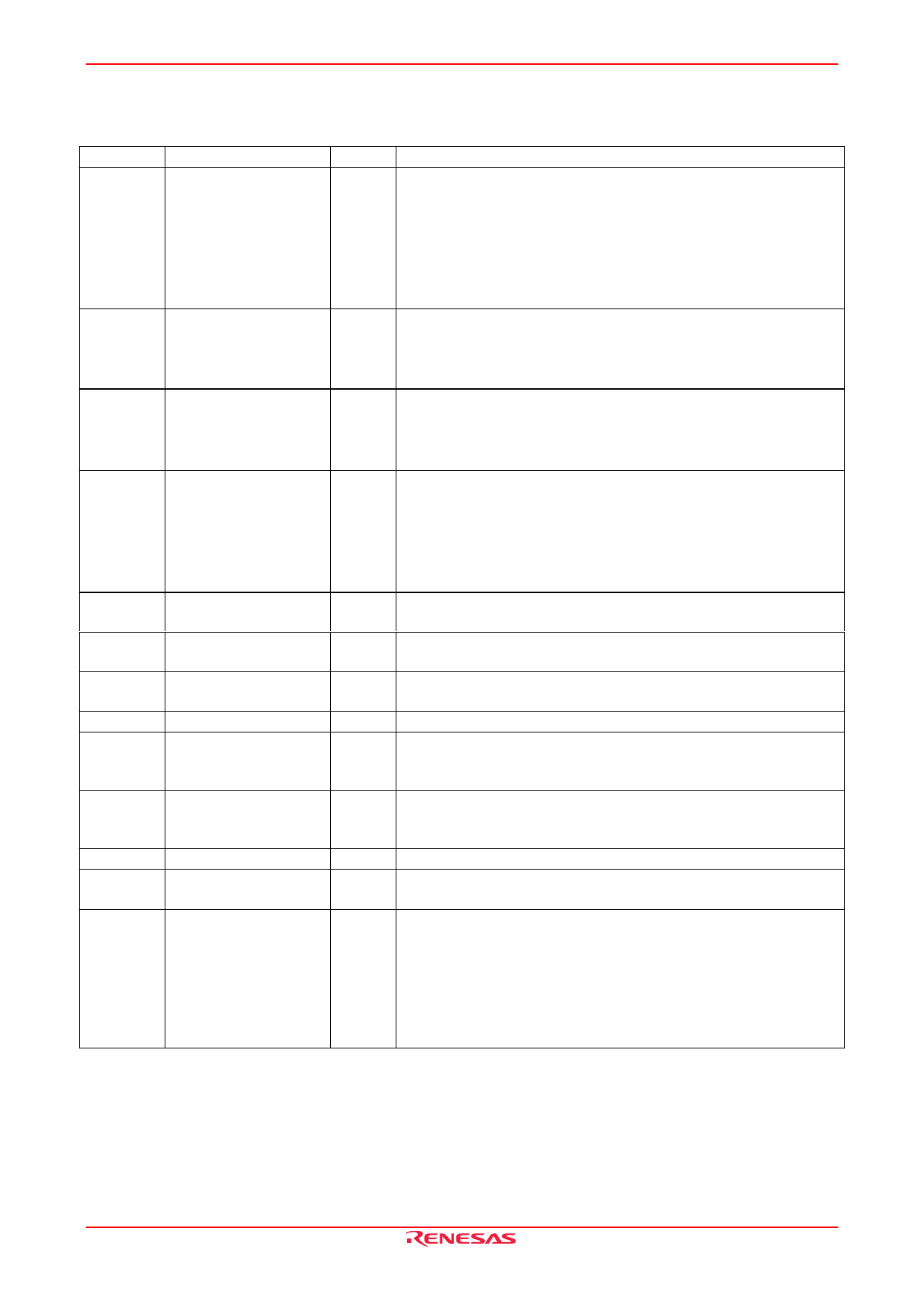
Register Configuration
List of Registers
Address
Register Name
R/W
Description
0
System setting
R/W
• LSI H/W reset
• Coding/decoding/image data through mode selection
• Context selection (internal context/external context)
• Byte swap ON/OFF of coded/image data on host bus
• Bit swap ON/OFF of coded/image data on host bus
• Image data I/O I/F (parallel I/F, serial I/F)
• Image data bus bit width selection (32 bits/16 bits)
1
Parameter setting
R/W
• Template selection (2-line/3-line template)
• Setting of AT pixel position (up to 127) (If 0 is set, AT becomes
non-existent (default position))
• Latch input/through input selection in external context input mode
2
Command
W
• Context table RAM initialization command
• Coding (decoding, through) start/end command
• Start/stop command for R/W of context table RAM
• Selection of temporary stop and terminating end
2
Status
R
• Processing status (in process/end of processing)
• Coded data read/write ready (ready/busy)
• Marker code detection (SDNORM, SDRST, ABORT, others)
• Interrupt request status
• SC counter overflow
• Processing mode (stop temporary/terminating end)
3
Interrupt enable setting R/W
• Interrupt enable setting correspondence to each of bits positions
of status register
4, 5
Pixel count setting
R/W
• Setting the number of pixels on one line (in multiples of 16 or 32,
up to 10240 pixels)
6, 7
Line count setting
R/W
• Setting the number of lines to be coded/decoded (up to 65535
lines)
8, 9
Processed line count R
• Setting the number of coded/decoded lines (up to 65535 lines)
A, B
Data write buffer
W
• Buffer for writing coded data/image data/context table RAM data
from MPU into LSI (DMA transferable) (RAM address is
automatically incremented each time data is written.)
A, B
Data read buffer
R
• Buffer for reading coded data/image data/context table RAM data
from LSI into MPU (DMA transferable) (RAM address is
automatically incremented each time data is read).
C
Marker code setting
W
• Setting a terminal marker code in coding (SDNORM/SDRST)
C
Marker code read
R
• Reading a marker code in decoding (SDNORM, SDRST, ABORT,
others)
D
Scaling
R/W
• Reduction in coding (1/2 reduction in horizontal and vertical
directions, horizontal OR processing)
• Magnification during decoding (×2 lengthwise and width)
• Select throwing away the leading 1-byte of the coded data read
when decoding
• Selecting the typical prediction
• Selection of prohibiting line memory initialization
Note: When the 8-bit bus is used for the data read/write buffer, use address A only.
Incase of the 16-bit buffer, only the word access is possible.
(The byte access is not possible.)
REJ03F0234-0200 Rev.2.00 Sep 14, 2007
Page 9 of 33
Share Link: 