IDT29FCT52A Просмотр технического описания (PDF) - Integrated Device Technology
Номер в каталоге
Компоненты Описание
Список матч
IDT29FCT52A Datasheet PDF : 7 Pages
| |||
IDT29FCT52A/B/C, IDT29FCT53A/B/C
FAST CMOS OCTAL REGISTERED TRANSCEIVERS
MILITARY AND COMMERCIAL TEMPERATURE RANGES
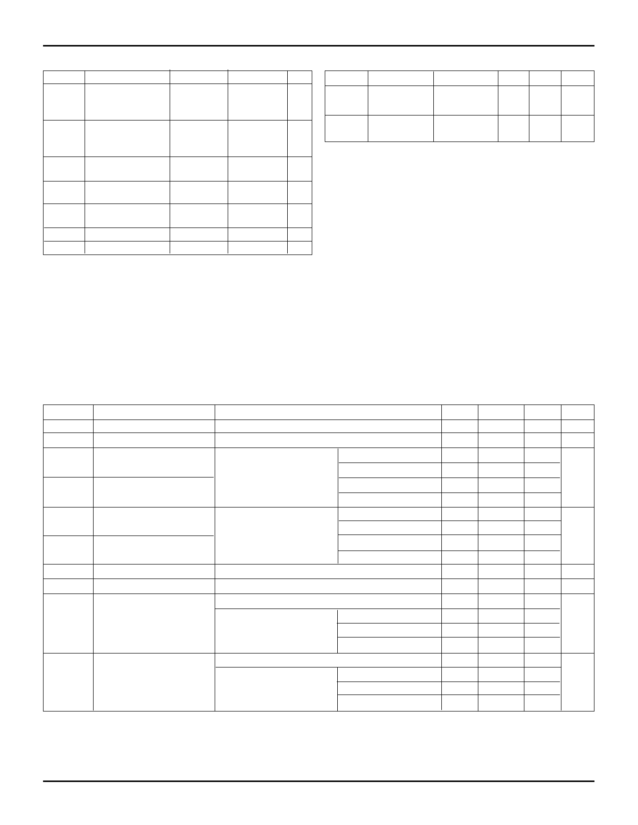
ABSOLUTE MAXIMUM RATINGS(1)
Symbol
Rating
VTERM(2) Terminal Voltage
with Respect
to GND
VTERM(3) Terminal Voltage
with Respect
to GND
Commercial Military Unit
–0.5 to +7.0 –0.5 to +7.0 V
–0.5 to VCC –0.5 to VCC V
TA
Operating
Temperature
0 to +70 –55 to +125 °C
TBIAS
Temperature
Under Bias
–55 to +125 –65 to +135 °C
TSTG
Storage
Temperature
–55 to +125 –65 to +150 °C
PT
Power Dissipation
0.5
0.5
W
IOUT
DC Output Current
120
120
mA
NOTES:
2533 tbl 04
1. Stresses greater than those listed under ABSOLUTE MAXIMUM
RATINGS may cause permanent damage to the device. This is a stress
rating only and functional operation of the device at these or any other
conditions above those indicated in the operational sections of this
specification is not implied. Exposure to absolute maximum rating
conditions for extended periods may affect reliability. No terminal voltage
may exceed +0.5V unless otherwise noted.
2. Inputs and VCC terminals only.
3. Outputs and I/O terminals only.
CAPACITANCE (TA = +25°C, f = 1.0MHz)
Symbol Parameter(1) Conditions Typ. Max. Unit
CIN
Input
VIN = 0V
Capacitance
6
10 pF
CI/O
I/O
VOUT = 0V
8
12 pF
Capacitance
NOTE:
2533 tbl 05
1. This parameter is guaranteed by characterization data and not tested.
DC ELECTRICAL CHARACTERISTICS OVER OPERATING RANGE
Following Conditions Apply Unless Otherwise Specified: VLC = 0.2V; VHC = VCC – 0.2V
Commercial: TA = 0°C to +70°C, VCC = 5.0V ± 5%; Military: TA = –55°C to +125°C, VCC = 5.0V ± 10%
Symbol
Parameter
Test Conditions(1)
Min. Typ.(2) Max. Unit
VIH
Input HIGH Level
Guaranteed Logic HIGH Level
2.0
—
—
V
VIL
Input LOW Level
Guaranteed Logic LOW Level
—
—
0.8
V
IIH
Input HIGH Current
VCC = Max.
(Except I/O Pins)
IIL
Input LOW Current
VI =VCC
VI = 2.7V
VI = 0.5V
—
—
5
µA
—
—
5(4)
—
—
–5(4)
(Except I/O Pins)
VI = GND
—
—
–5
IIH
Input HIGH Current
VCC = Max.
(I/O Pins Only)
IIL
Input LOW Current
VI = VCC
VI = 2.7V
VI = 0.5V
—
—
15
µA
—
—
15(4)
—
—
–15(4)
(I/O Pins Only)
VI = GND
—
—
–15
VIK
Clamp Diode Voltage
Vcc = Min., IN = –18mA
IOS
Short Circuit Current
Vcc = Max.(3), VO = GND
—
–0.7 –1.2 V
–60
–120
—
mA
VOH
Output HIGH Voltage
Vcc = 3V, VIN = VLC or VHC, IOH = –32µA
VHC
VCC
—
V
Vcc = Min.
IOH = –300µA
VHC
VCC
—
VIN = VIH or VIL
IOH = –15mA MIL.
2.4
4.0
—
IOH = –24mA COM’L. 2.4
4.0
—
VOL
Output LOW Voltage
Vcc = 3V, VIN = VLC or VHC, IOL = 300µA
—
GND VLC
V
Vcc = Min.
IOL = 300µA
—
GND VLC(4)
VIN = VIH or VIL
IOL = 48mA MIL.(5)
—
0.3 0.55
IOL = 64mA COM’L.(5)
—
0.3 0.55
NOTES:
2533 tbl 06
1. For conditions shown as Max. or Min., use appropriate value specified under Electrical Characteristics for the applicable device type.
2. Typical values are at VCC = 5.0V, +25°C ambient and maximum loading.
3. Not more than one output should be shorted at one time. Duration of the short circuit test should not exceed one second.
4. This parameter is guaranteed but not tested.
5. These are maximum IOL values per output, for 8 outputs turned on simultaneously. Total maximum IOL (all outputs) is 512mA for commercial and
384mA for military. Derate IOL for number of outputs exceeding 8 turned on simultaneously.
7.1
3
Share Link: 