W48S87-04(1999) Просмотр технического описания (PDF) - Cypress Semiconductor
Номер в каталоге
Компоненты Описание
Список матч
W48S87-04 Datasheet PDF : 21 Pages
| |||
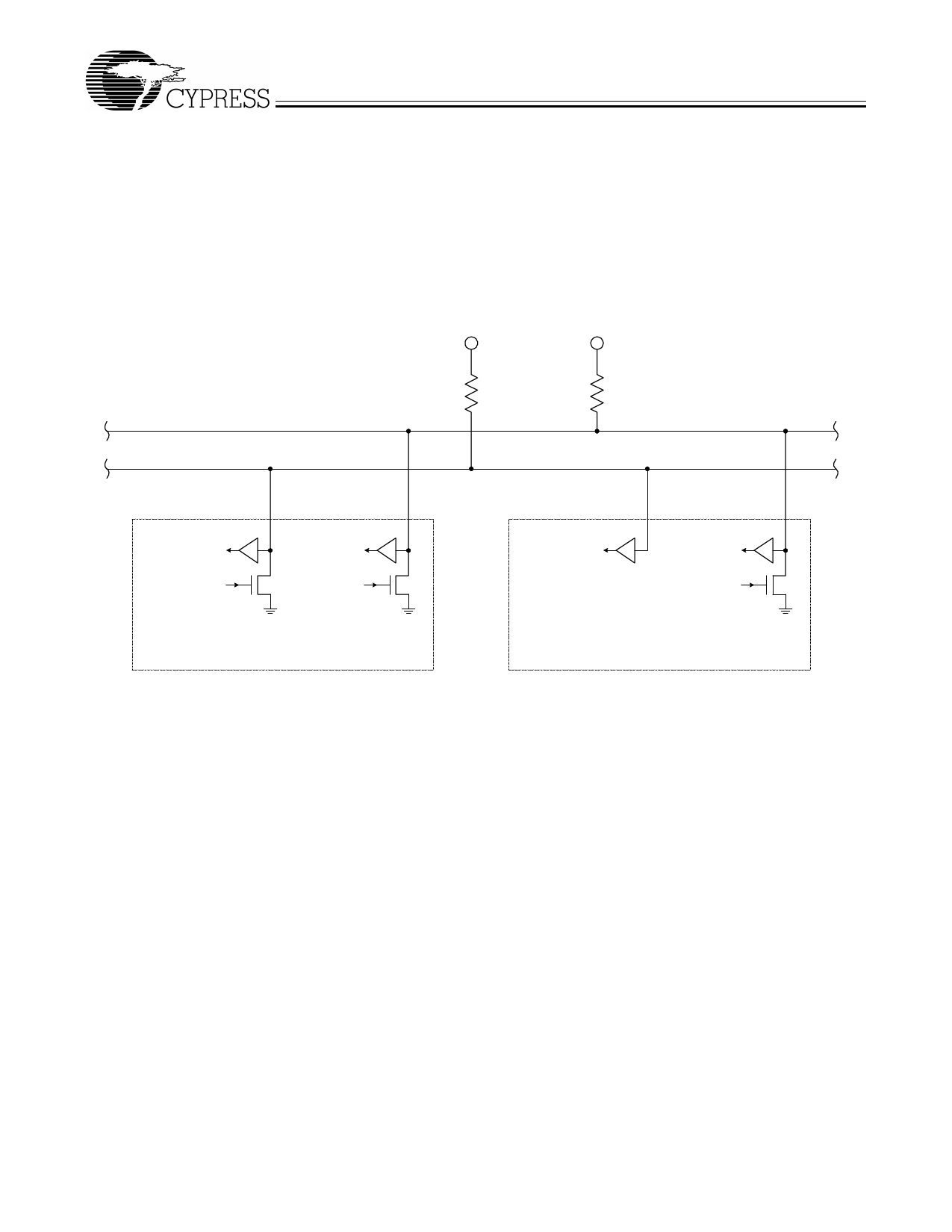
PRELIMINARY
Table 4. Data Bytes 0–6 Serial Configuration Map (continued)
Affected Pin
Bit(s) Pin No. Pin Name
Control Function
Data Byte 3
7
28
SDRAM7 Clock Output Disable
6
29
SDRAM6 Clock Output Disable
5
31
SDRAM5 Clock Output Disable
4
32
SDRAM4 Clock Output Disable
3
34
SDRAM3 Clock Output Disable
2
35
SDRAM2 Clock Output Disable
1
37
SDRAM1 Clock Output Disable
0
38
SDRAM0 Clock Output Disable
Data Byte 4
7
--
--
(Reserved)
6
--
--
(Reserved)
5
--
--
(Reserved)
4
--
--
(Reserved)
3
17
SDRAM11 Clock Output Disable
2
18
SDRAM10 Clock Output Disable
1
20
SDRAM9 Clock Output Disable
0
21
SDRAM8 Clock Output Disable
Data Byte 5
7
--
--
(Reserved)
5
--
--
(Reserved)
5
--
--
(Reserved)
4
47
IOAPIC Clock Output Disable
3
--
--
(Reserved)
2
--
--
(Reserved)
1
46
REF1 Clock Output Disable
0
2
REF0 Clock Output Disable
Data Byte 6
7
--
--
(Reserved)
6
--
--
(Reserved)
5
--
--
(Reserved)
4
--
--
(Reserved)
3
--
--
(Reserved)
2
--
--
(Reserved)
1
--
--
(Reserved)
0
--
--
(Reserved)
Bit Control
0
1
Low
Active
Low
Active
Low
Active
Low
Active
Low
Active
Low
Active
Low
Active
Low
Active
--
--
--
--
--
--
--
--
Low
Active
Low
Active
Low
Active
Low
Active
--
--
--
--
--
--
Low
Active
--
--
--
--
Low
Active
Low
Active
--
--
--
--
--
--
--
--
--
--
--
--
--
--
--
--
W48S87-04
Default
1
1
1
1
1
1
1
1
0
0
0
0
1
1
1
1
0
0
0
1
0
0
1
1
0
0
0
0
0
0
0
0
9
Share Link: 