W83194BR-63S Просмотр технического описания (PDF) - Winbond
Номер в каталоге
Компоненты Описание
Список матч
W83194BR-63S Datasheet PDF : 16 Pages
| |||
W83194BR-63S
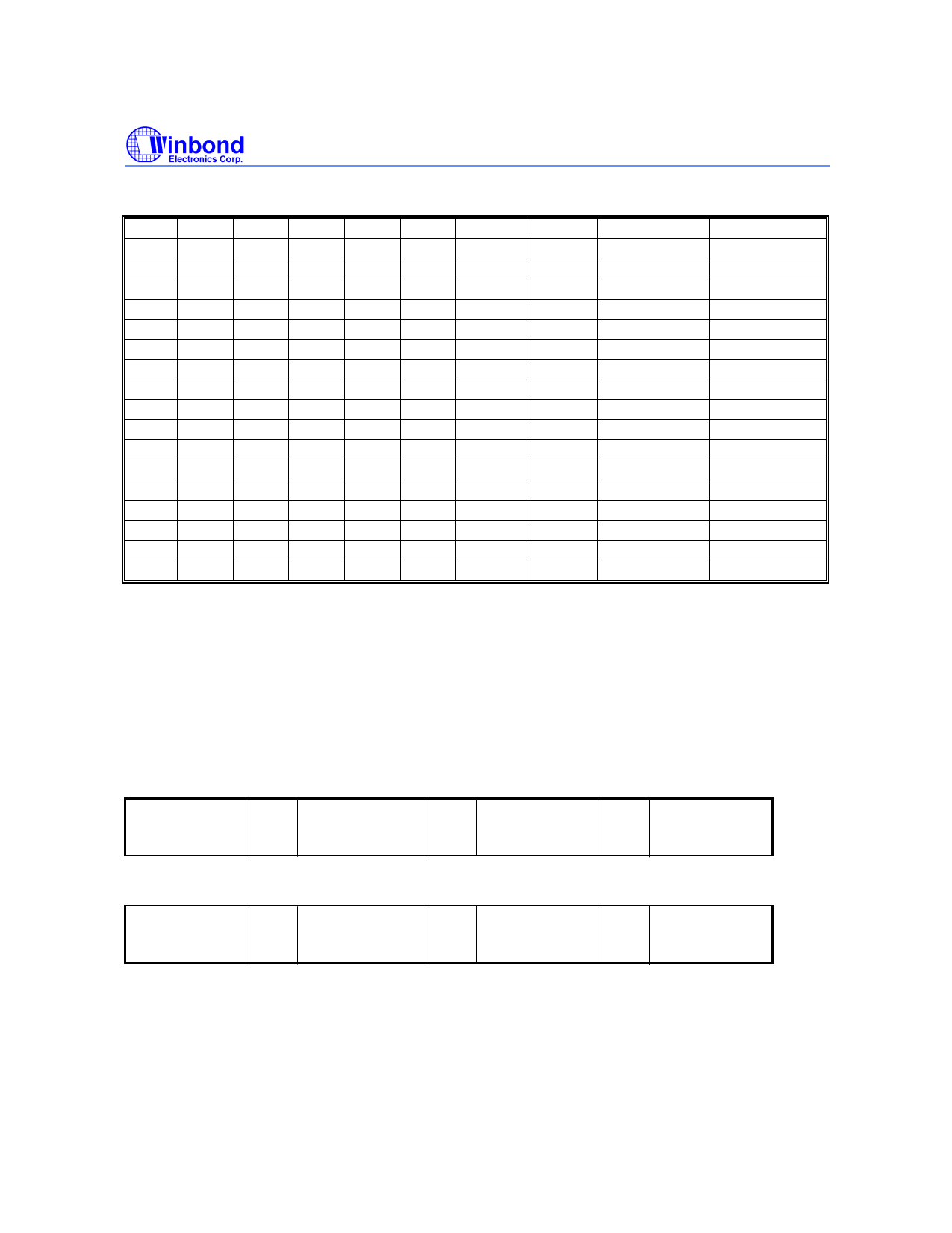
5. FREQUENCY SELECTION BY HARDWARE
VCO CPU SDRAM PCI
FS3 FS2 FS1 FS0 (MHz) (MHz) (MHz) (MHz)
0
0
0
0
400 66.6 66.6
33.3
0
0
0
1 400 100 100
33.3
0
0
1
0 498 166 166 31.25
0
0
1
1 400 133.3 133.3 33.3
0
1
0
0 400 66.6 100
33.3
0
1
0
1
400 100 66.6
33.3
0
1
1
0 400 100 133
33.3
0
1
1
1 400 133.3 100
33.3
1
0
0
0 336 112 112
33.6
1
0
0
1 372 124 124
31
1
0
1
0 414 138 138
34.5
1
0
1
1 300 150 150
30
1
1
0
0 399.6 66.6 133
33.3
1
1
0
1 300 100 150
30
1
1
1
0 300 150 100
30
1
1
1
1 480 160 120
30
AGPSEL=0
(MHz)
66.6
66.6
62.5
66.6
66.6
66.6
66.6
66.6
67.2
62
69
60
66.6
60
60
60
AGPSEL=1
(MHz)
50
50
50
50
50
50
50
50
56
46.5
51.8
50
50
50
50
48
6. SERIAL CONTROL REGISTERS
The Pin column lists the affected pin number and the @PowerUp column gives the default state at
true power up. "Command Code" byte and "Byte Count" byte must be sent following the
acknowledge of the Address Byte. Although the data (bits) in these two bytes are considered "don't
care", they must be sent and will be acknowledge. After that, the sequence described below
(Register 0, Register 1, Register 2, ....) will be valid and acknowledged.
Bytes sequence order for I2C controller :
Clock Address
A(6:0) & R/W
Ack
8 bits dummy
Command code
Ack
8 bits dummy
Byte count
Ack
Byte0,1,2...
until Stop
Set R/W to 1 when Read back”, the data sequence is as follows :
Clock Address
A(6:0) & R/W
Ack
Byte 0
Ack
Byte 1
Ack
Byte2, 3, 4...
until Stop
-6-
Share Link: 