UPD72012 Просмотр технического описания (PDF) - NEC => Renesas Technology
Номер в каталоге
Компоненты Описание
Список матч
UPD72012 Datasheet PDF : 36 Pages
| |||
µPD72012
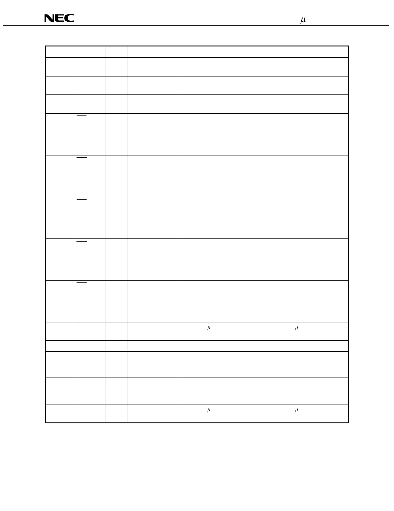
Pin No.Note 1 Pin Name
I/O
Signal Name
Function
(3/3)
31(37) CLKSEL
I
CLK SELECT
Pin for selecting whether to use 48 MHz oscillator or 4 MHz crystal
oscillator (refer to Table 1-1).
32(38)
DVDD
(Buffer)
-
DVDD
(Buffer)
Connect to 3.3 V power supply.
(39)
DVDD
-
DVDD
Connect to 3.3 V power supply. This pin is used together with pin No.
32 internally in the shrink DIP product.
33(40) PP1
O PORTPOWER#1 Low active open drain output pin that controls downstream port #1
power supply.
Input the output of this pin to the power control element of an external
circuit.
If not using this pin, leave it unconnected. Note 2
34(41) PP2
O PORTPOWER#2 Low active open drain output pin that controls downstream port #2
power supply.
Input the output of this pin to the power control element of an external
circuit.
If not using this pin, leave it unconnected. Note 2
35(42) PP3
O PORTPOWER#3 Low active open drain output pin that controls downstream port #3
power supply.
Input the output of this pin to the power control element of an external
circuit.
If not using this pin, leave it unconnected. Note 2
36(43) PP4
O PORTPOWER#4 Low active open drain output pin that controls downstream port #4
power supply.
Input the output of this pin to the power control element of an external
circuit.
If not using this pin, leave it unconnected. Note 2
37(44) PP5
O PORTPOWER#5 Low active open drain output pin that controls downstream port #5
power supply.
Input the output of this pin to the power control element of an external
circuit.
If not using this pin, leave it unconnected. Note 2
38(1)
DVDD
-
DVDD
(TS0)
Test pin of µPD72012 (corresponds to TS0 pin in µPD72011).
Connect to 3.3 V power supply.
39(2)
DGND
-
DGND
Connect to GND.
40(3)
PSSEL
I
Power SW
Pin that selects switching between bus power and self-power (refer to
Table 1-2).
To make high level, pull up to 3.3 V.
41(4)
PVSEL
I
Port Value
Pin that selects switching between number (4 or 5) of downstream
ports (refer to Table 1-2).
To make high level, pull up to 3.3 V.
42(5)
DGND
-
DGND
(TS2)
Test pin of µPD72012 (corresponds to TS2 pin in µPD72011).
Connect to GND.
Notes 1. QFP pin numbers are shown in ( ).
2. For details, refer to Table 1-4 of 1.2 Tables by Pin Function.
Data Sheet S13918EJ3V0DS
9
Share Link: 