UPD72012 Просмотр технического описания (PDF) - NEC => Renesas Technology
Номер в каталоге
Компоненты Описание
Список матч
UPD72012 Datasheet PDF : 36 Pages
| |||
µPD72012
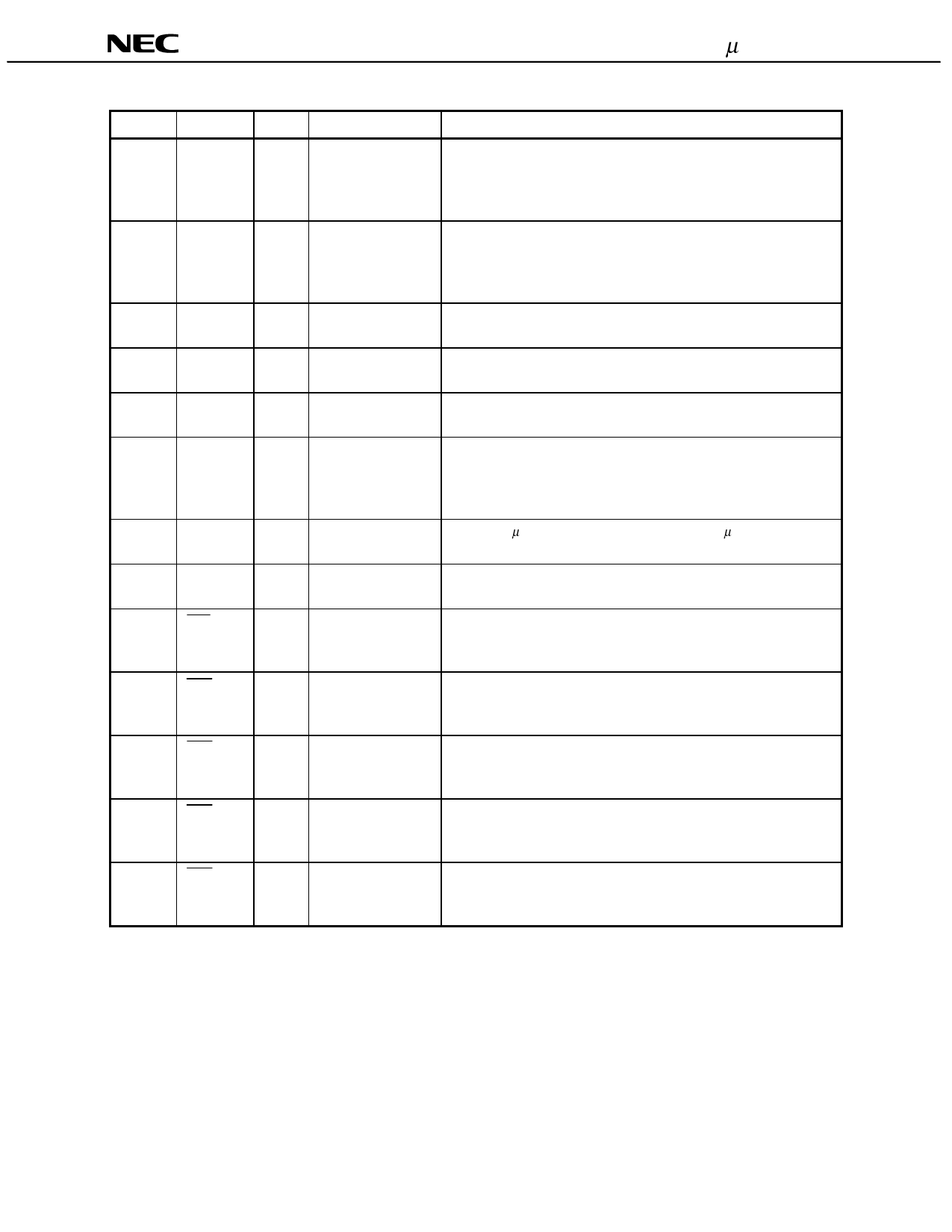
Pin No.Note 1 Pin Name
I/O
Signal Name
Function
(2/3)
18(24)
AVDD1
-
AVDD1
Power supply pin of on-chip clock drive circuit.
To stabilize the power supply, connect directly to a stable power
supply using the shortest wire possible or connect to GND via a
capacitor along the wire (3.3 V input).
19(25) CLK / X2
I
CLOCK / XTAL
When you input a clock signal from an oscillator, input at the 48 MHz
CMOS level (5 V can be input).
When using a 4 MHz crystal oscillator, connect the oscillator to this
pin.
20(26) X1
I
XTAL
When using a 4 MHz crystal oscillator, connect the oscillator to this
pin.
21(27) AGND1
-
AGND1
GND pin of on-chip clock drive circuit.
Connect to GND.
22(28) AGND2
-
AGND2
GND pin of on-chip frequency multiplier (PLL).
Connect to GND.
23(29)
AVDD2
-
AVDD2
Power supply pin of on-chip frequency multiplier (PLL).
To stabilize the power supply, connect directly to a stable power
supply using the shortest wire possible or connect to GND via a
capacitor along the wire (3.3 V input).
24(30)
DVDD
-
DVDD
(TS1)
Test pin of µPD72012 (corresponds to TS1 pin in µPD72011).
Connect to 3.3 V power supply.
25(31)
DGND
(Buffer)
-
DGND
(Buffer)
Connect to GND.
26(32) CS1
I
PORTCURRENT1 Low active input pin that inputs overcurrent states detected by
external circuit of downstream port #1.
When not using this pin, connect it directly to VDD. Note 2
27(33) CS2
I
PORTCURRENT2 Low active input pin that inputs overcurrent states detected by
external circuit of downstream port #2.
When not using this pin, connect it directly to VDD. Note 2
28(34) CS3
I
PORTCURRENT3 Low active input pin that inputs overcurrent states detected by
external circuit of downstream port #3.
When not using this pin, connect it directly to VDD. Note 2
29(35) CS4
I
PORTCURRENT4 Low active input pin that inputs overcurrent states detected by
external circuit of downstream port #4.
When not using this pin, connect it directly to VDD. Note 2
30(36) CS5
I
PORTCURRENT5 Low active input pin that inputs overcurrent states detected by
external circuit of downstream port #5.
When not using this pin, connect it directly to VDD. Note 2
Notes 1. Pin numbers for QFP are shown in ( ).
2. For details, refer to Table 1-3 in 1.2 Tables by Pin Function.
8
Data Sheet S13918EJ3V0DS
Share Link: 